Plasma display panel

a technology of plasma and display panel, which is applied in the direction of discharge tube luminescnet screen, instrument, electrode, etc., can solve the problems of permanent latent image reduction, low light emission efficiency, and reduced area for coating phosphor, so as to increase the discharge space, increase the visible light emission area, and reduce the effect of driving voltag

Inactive Publication Date: 2006-06-08
SAMSUNG SDI CO LTD
View PDF16 Cites 1 Cited by
  • Summary
  • Abstract
  • Description
  • Claims
  • Application Information

AI Technical Summary

Benefits of technology

[0013] The present invention provides a plasma display panel having a structure which increases a discharge space, increases a visible light emission area, and enables a low driving voltage to increase brightness and light emission efficiency.

Problems solved by technology

The alternating current type, three-electrode surface discharge PDP has a drawback in that only approximately 60% of visible light generated by the phosphor layer is emitted since a considerable amount of the visible light is absorbed by the dielectric layer covering the sustain electrode pairs on the lower surface of the front substrate, thereby providing a low light emission efficiency.
Also, the alternating current type, three-electrode surface discharge PDP has a problem of permanent latent images due to ion sputtering of charged discharge gas particles onto the phosphor layer after prolonged operation.
However, when the height of the barrier ribs is reduced, the area for coating phosphor is also reduced, thereby reducing the overall brightness of the panel.

Method used


Image

  • Plasma display panel
  • Plasma display panel
  • Plasma display panel

Examples


Embodiment Construction

[0024] The present invention will now be described more fully with reference to the accompanying drawings, in which exemplary embodiments of the invention are shown.

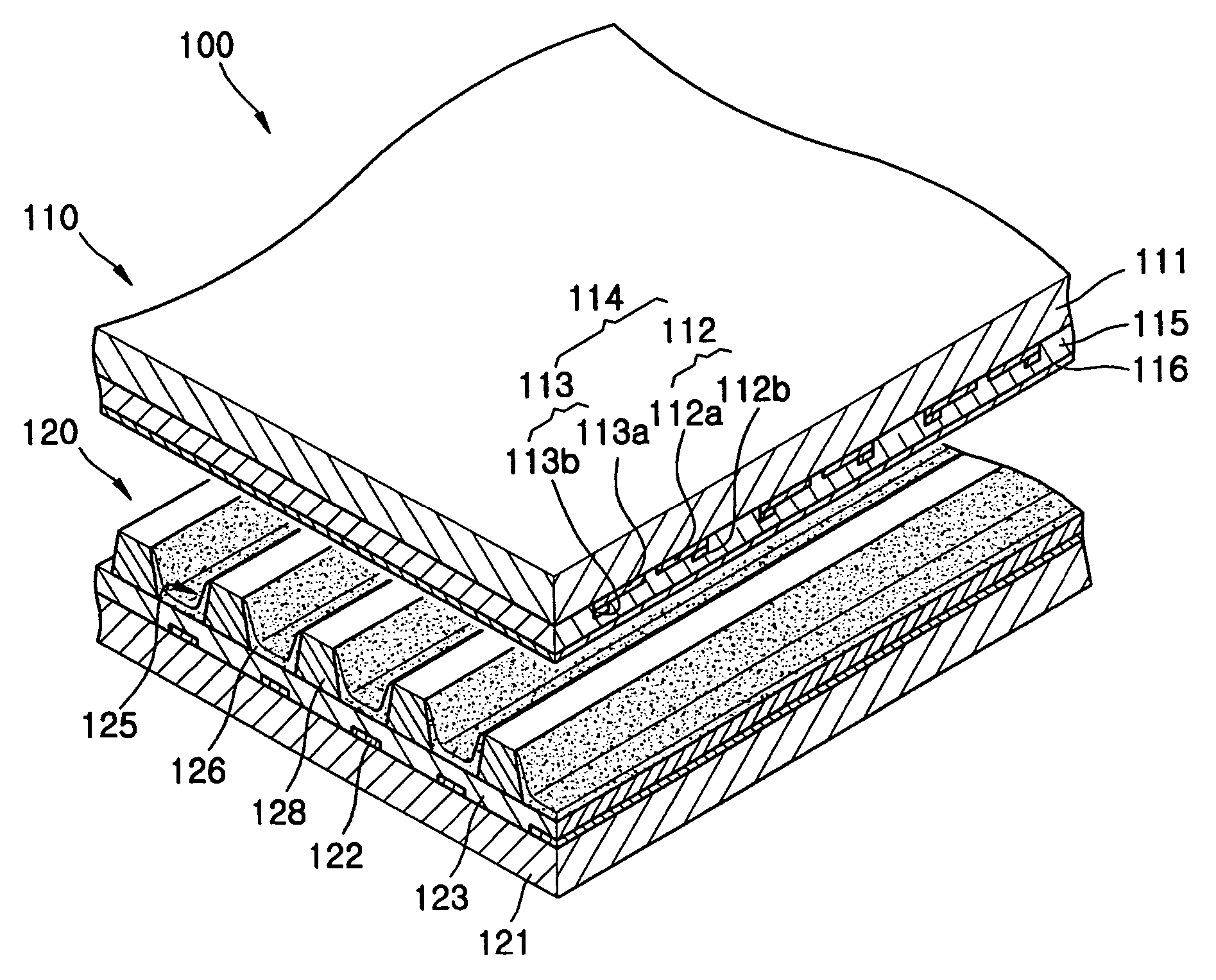
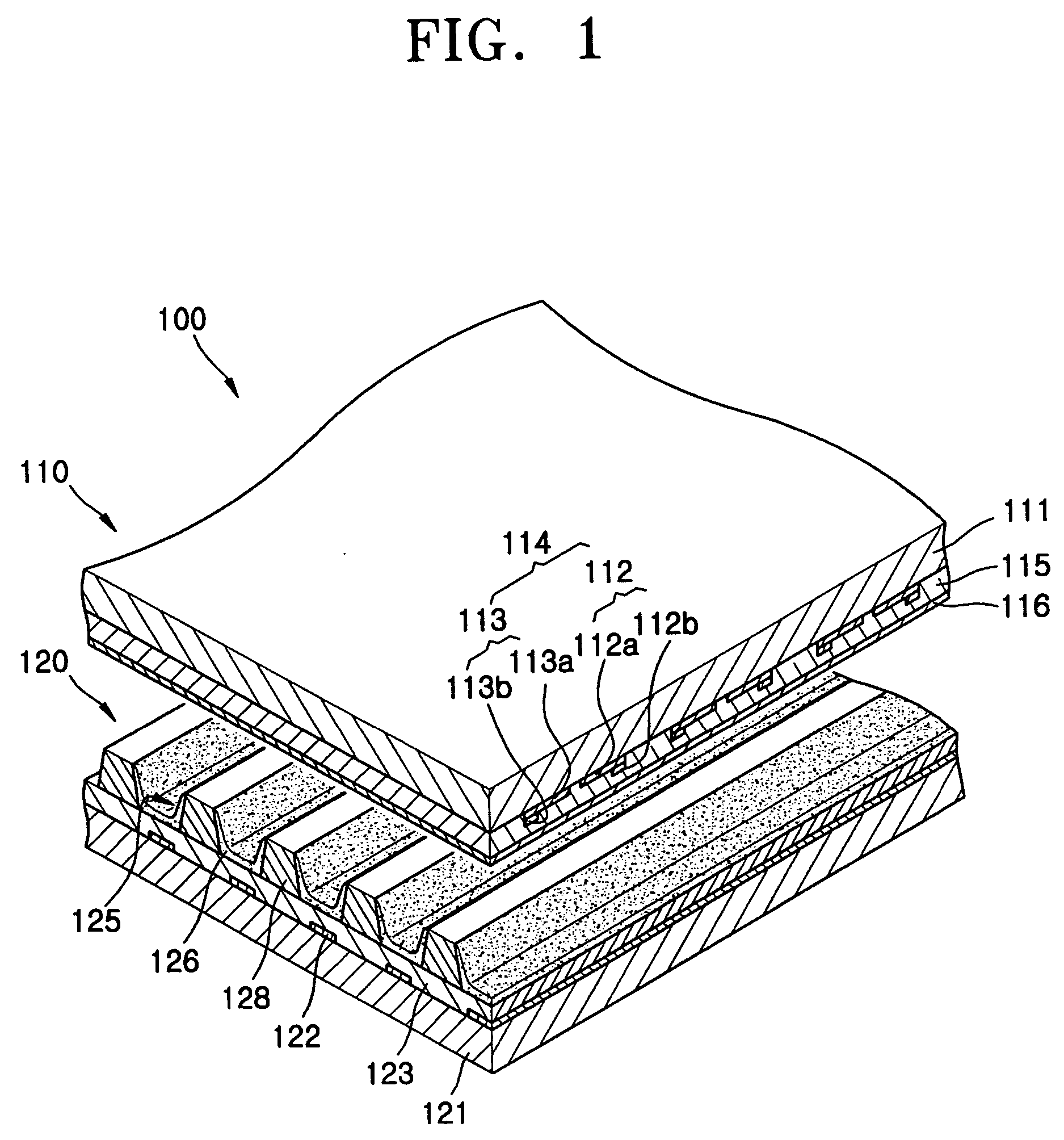
[0025]FIG. 1 is a perspective view of a plasma display panels (PDP). More specifically, an alternating current type, three-electrode surface discharge PDP is shown.

[0026] The PDP 100 typically includes a front panel 110 and a rear panel 120. The front panel 110 includes a front substrate 111, a plurality of sustain electrode pairs 114 each having a Y electrode 112 and an X electrode 113 formed on a lower surface of the front substrate 111, a front dielectric layer 115 covering the sustain electrode pairs 114, and a protection film 116 which covers the front dielectric layer 115. The X electrode 113 and the Y electrode 112 include transparent electrodes 112a and 113a, respectively, formed of indium tin oxide (ITO) and bus electrodes 112b and 113b, respectively, formed of a highly conductive metal.

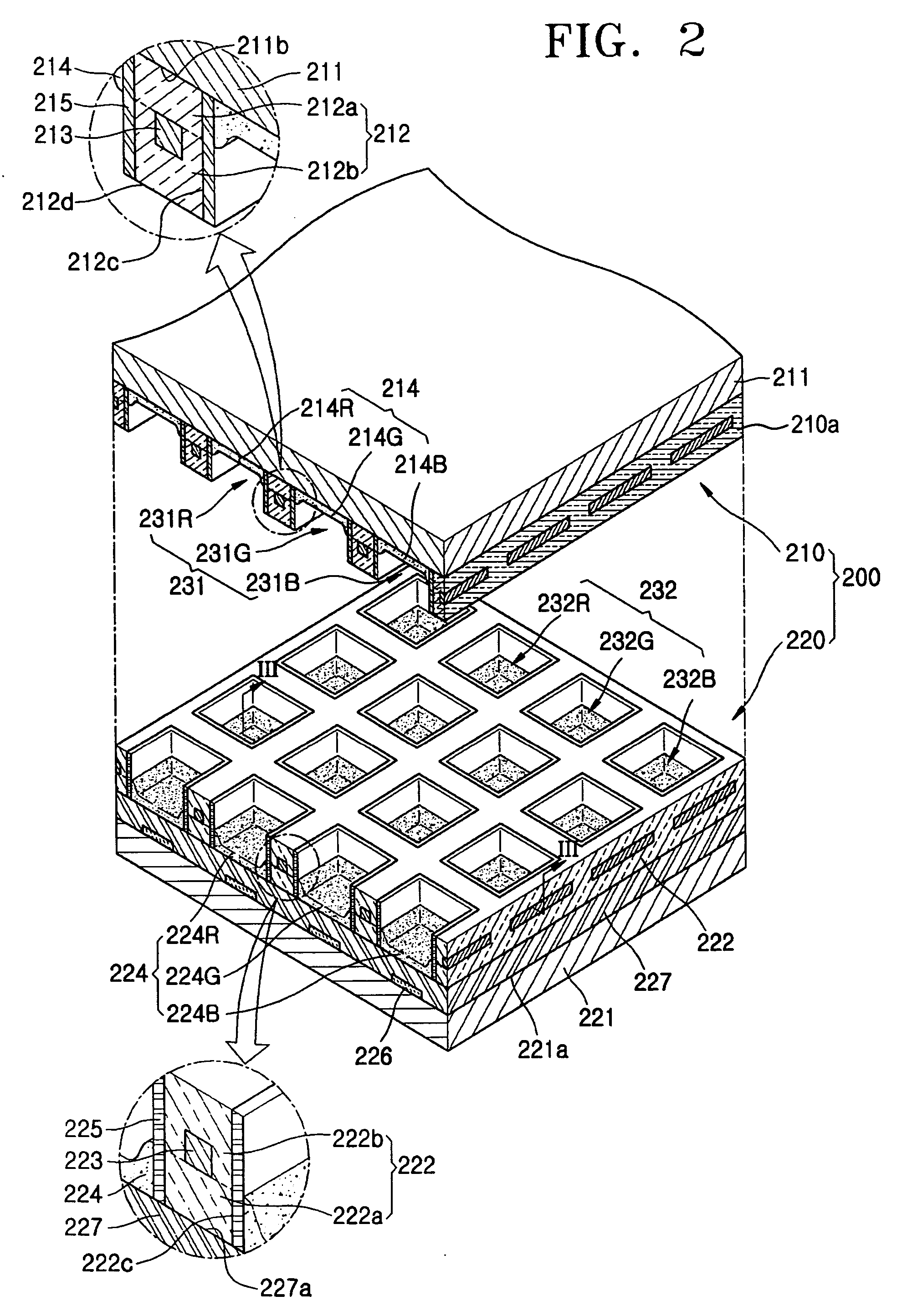
[0027] The rear panel ...


PUM


Abstract

A plasma display panel (PDP) has a structure which extends a discharge space, increases a visible light emission area, enables a low driving voltage, and improves light emission efficiency. The PDP comprises: a pair of substrates including a first substrate and a second substrate facing each other; a barrier rib located between the first substrate and the second substrate, and defining discharge, together with the first and second substrates, cells where gas discharge is generated; a plurality of discharge electrodes comprising first discharge electrodes and second discharge electrodes, surrounding the discharge cell vertically spaced in the barrier rib, for generating a gas discharge by mutual actions; and a first phosphor layer and a second phosphor layer located in the discharge cell formed in the first substrate and in the discharge cell formed in the second substrate, respectively.

Description

CLAIM OF PRIORITY [0001] This application makes reference to, incorporates the same herein, and claims all benefits accruing under 35 U.S.C. §119 from an application for PLASMA DISPLAY PANEL earlier filled in the Korean Intellectual Property Office on 8 Dec. 2004 and there duly assigned Serial No. 10-2004-0103131. BACKGROUND OF THE INVENTION [0002] 1. Technical Field [0003] The present invention relates to a plasma display panel, and more particularly, to a plasma display panel having a structure which increases a discharge space and a visible light emitting area, and enables low voltage driving, so as to increase brightness and improve light emission efficiency. [0004] 2. Description of the Related Art [0005] Plasma display panels (PDPs) have received considerable attention as the next generation of flat display devices due to their superior characteristics, such as large screen size, high image quality, ultrathin and lightweight design, large viewing angle, simple manufacturing pr...

Claims


Application Information

Patent Timeline
Patent Type & Authority Applications(United States)
IPC IPC(8): G09G3/10H01J11/12H01J11/16H01J11/24H01J11/26H01J11/32H01J11/36H01J11/38H01J11/40H01J11/42H01J11/50
CPCH01J11/16H01J11/24H01J11/32H01J2211/323H01J11/22H01J11/42
Inventor KIM, SE-JONG
Owner SAMSUNG SDI CO LTD
Why Eureka
Try Eureka