Display apparatus, digital-to-analog conversion circuit and digital-to-analog conversion method

a technology of digital to analog conversion and display apparatus, applied in the direction of instruments, cathode-ray tube indicators, computing, etc., can solve the problems of deterioration in display quality, difficult technical processing of tft with uniform characteristics on glass substrate, and inability to operate at very fast speed

Inactive Publication Date: 2006-06-08
JAPAN DISPLAY CENT INC
View PDF9 Cites 10 Cited by
  • Summary
  • Abstract
  • Description
  • Claims
  • Application Information

AI Technical Summary

Benefits of technology

[0014] It is an object of the present invention to provide

Problems solved by technology

However, since the operation speed of the TFT formed on the glass substrate is not very fast, various kinds of ingenuity of circuits are required in order to constitute the drive circuit.
Further, forming the TFT with the uniform characteristics on the glass substrate is technically difficult at the present moment, and deterioration in display quality, e.g., irregularities in display may occur due to a difference in characteristics of the TFTs.
Furthermore, when the pixel array portion and the drive circuit are formed on the same glass substrate, a percentage of the pixel ar

Method used


Image

  • Display apparatus, digital-to-analog conversion circuit and digital-to-analog conversion method
  • Display apparatus, digital-to-analog conversion circuit and digital-to-analog conversion method
  • Display apparatus, digital-to-analog conversion circuit and digital-to-analog conversion method

Examples


second embodiment

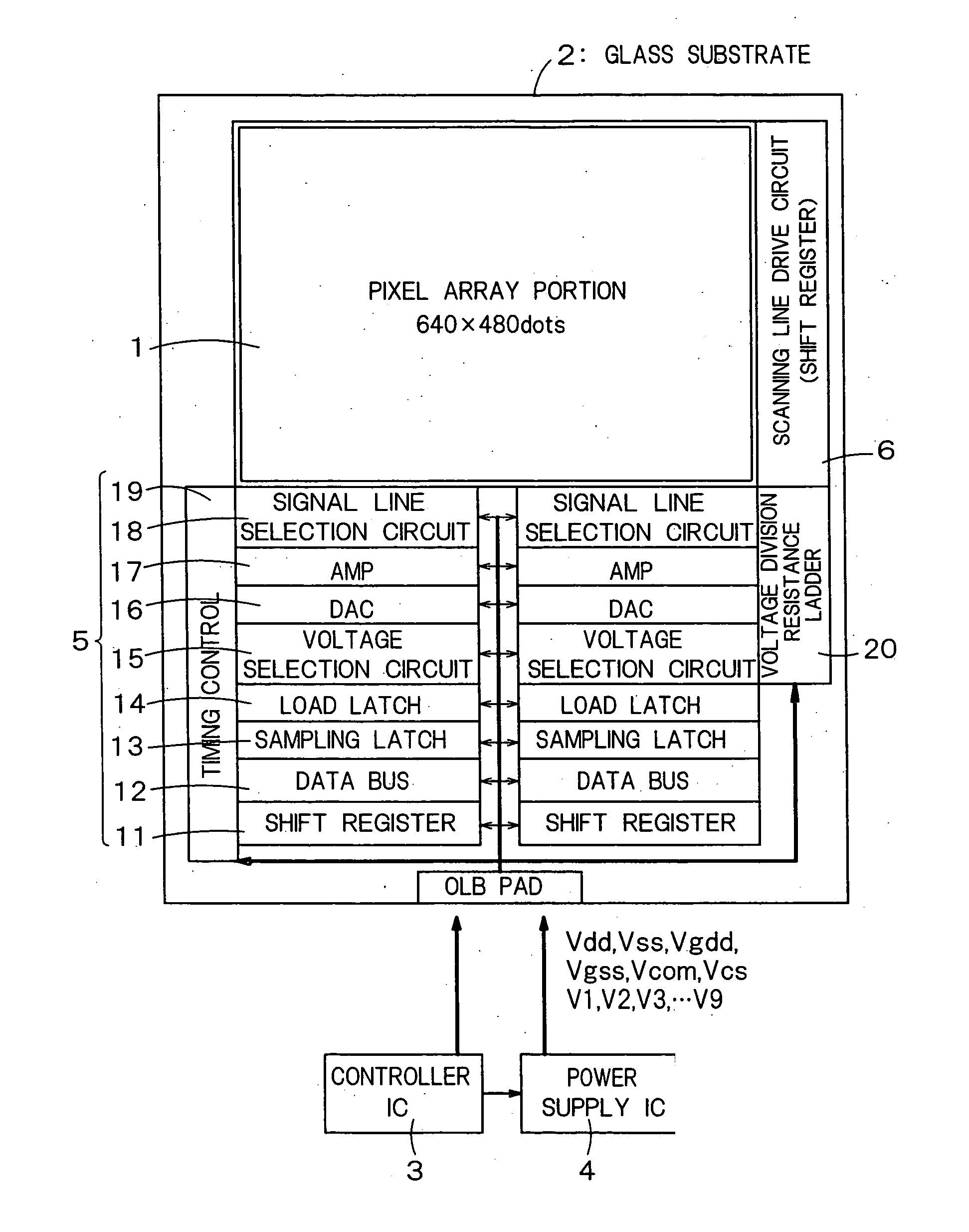
[0214] The signal line selection circuit 18 in the signal line drive circuit 5 is constituted by an analog switch consisting of a TFT. However, the ON resistance of the analog switches varies due to irregularities in characteristic of the TFT, and irregularities in drive speed of the signal line by the AMP may lead to display irregularities.

[0215] Additionally, if local irregularities in Vth occur, the ON resistance of a specific analog switch becomes too small, the loop of the cascade-connected inverters on the odd number of stages gets close to the no-load state, and oscillation of the AMP is caused. As a result, a line defect may be possibly generated.

[0216] Thus, as shown in FIG. 6A, the signal line selection circuit 18 may be constituted by connecting two analog switches S21 and S22 in parallel in accordance with each signal line. In this case, in regard to the circuit diagram of the signal line selection circuit 18 connected to a given signal line, the analog switches S21 an...

third embodiment

[0219] It is technically difficult to uniformize the ON resistances of the analog switches constituting the signal line selection circuit 18. Thus, as shown in FIG. 7, there can be considered a technique that a resistance element R5 is inserted between the signal line selection circuit 18 and the signal line in order to reduce the influence of the ON resistances of the analog switches in the signal line selection circuit 18. In this case, it is desirable that a resistance value of the resistance element R5 is set to a value larger than ON resistances of the analog switches in the signal line selection circuit 18. As a result, the impedance when seeing the signal line side from the AMP 17 side becomes dependent on the resistance value of the resistance element and unconcerned with the ON resistances of the analog switches in the signal line selection circuit 18, thereby reducing irregularities in signal line write timing.

[0220] Furthermore, a pre-charge control circuit 22 may be con...

fourth embodiment

[0223] As shown in FIG. 9A, the analog switch used in each portion in the signal line drive circuit 5 usually has a structure in which the NMOS transistor and the pMOS transistor are connected to each other in parallel. In case of this structure, however, when the analog switch enters the off state from the on state, the electric charge stored in the capacitance between the gate and the source of the analog switch flows into the load capacitance, and an output voltage of the analog switch disadvantageously fluctuates.

[0224] Here, assuming that respective gate-source capacitances of the PMOS transistor and the RMOS transistor when the analog switch is in the on state are Cgsp (ON) and Cgsn (ON) and respective gate-source capacitances of the pMOS transistor and the nMOS transistor when the analog switch is in the off state are Cgsp (OFF) and Cgsn (OFF), a quantity of fluctuation of the output voltage of the analog switch can be represented by the following expression (1). Δ⁢ ⁢V={Cgs...


PUM


Abstract

A signal line drive circuit according to the present invention has: a latch circuit which latches digital pixel data; a D/A converter which converts a latch output from the latch circuit into an analog video signal; an AMP which amplifies the analog video signal converted by the D/A converter; and a signal selection circuit which selects a signal line to which the analog video signal amplified by the AMP is supplied. The AMP has: an odd number of inverters which are cascade-connected; capacitor elements which are respectively connected between stages of the inverters and between an input terminal of the inverter on a first stage and an output terminal of the inverter on a last stage; a first power supply line which supplies a power supply voltage to the inverter on the first stage; and a second power supply line which supplies a power supply voltage to inverters other than the inverter on the first stage. The accuracy of the AMP can be improved by separating the power supply line for only the inverter on the first stage.

Description

CROSS REFERENCE TO RELATED APPLICATIONS [0001] This application is based upon and claims the benefit of priority from the prior Japanese Patent Applications No. 2001-132969 filed on Apr. 27, 2001, No. 2001-148175 filed on May 17, 2001 and No. 2001-400089 filed on Dec. 28, 2001, the entire contents of which are incorporated herein by reference. BACKGROUND OF THE INVENTION [0002] 1. Field of the Invention [0003] The present invention relates to a D / A converter which converts digital pixel data into analog video signals, a display apparatus in which an amplifier for amplifying an output from the D / A converter and a signal line selection circuit are formed integrally with a pixel array portion on an insulation substrate, a digital-to-analog conversion circuit for converting a digital signal into an analog signal, and a digital-to-analog conversion method. [0004] 2. Related Background Art [0005] A liquid display apparatus having a pixel array portion and a drive circuit formed on the sam...

Claims


Application Information

Patent Timeline
IPC IPC(8): G09G3/36G09G3/20H03M1/80
CPCG09G3/2011G09G3/3688G09G2300/0408G09G2310/0248G09G2310/027G09G2310/0291G09G2310/0297G09G2320/0233G09G2330/02G09G2330/021H03M1/804
Inventor NAKAMURA, TAKASHIHAYASHI, HIROTAKAFUJIWARA, HISAOKARUBE, MASAONAKAMURA, KAZUOKITANI, MASAKATSU
Owner JAPAN DISPLAY CENT INC
Why Eureka
Try Eureka