Stacked storage capacitor structure for a thin film transistor liquid crystal display

a technology of liquid crystal display and storage capacitor, which is applied in the direction of optics, semiconductor devices, instruments, etc., can solve the problems of reducing the area available on each pixel of such displays for the fabrication of storage capacitors, reducing the size of storage capacitors, and significantly affecting the performance of the overall lcd display. achieve the effect of increasing the overall capacitance of storage capacitors, reducing the area available on each pixel of such displays, and improving utilization

Active Publication Date: 2006-06-08
AU OPTRONICS CORP
View PDF6 Cites 47 Cited by
  • Summary
  • Abstract
  • Description
  • Claims
  • Application Information

AI Technical Summary

Benefits of technology

[0005] It is a primary objective of the present invention to increase the charge storage capacity without significantly affecting the aperture ratio in a pixel. The present invention is directed to better utilization of all layers of conductors and insulators for the fabrication of a storage capacitor in an associated pixel of an a-Si TFT-LCD array without changing the currently used fabrication processes for such a-Si TFT-LCD's. To accomplish this result, the source drain metal (M2) is used as a shared capacitor plate in a stacked capacitor structure comprising an MIM structure and a modified MII structure connected in

Problems solved by technology

In particular, it is well known that as the display resolution increases, the area available on each pixel of such displays for the fabrication of the storage capacitor is diminished due to aperture ratio considerations.
As a result, as the resolution of a-Si TFT-LCD's has increased, the size of the storage capacitor is reduced t

Method used


Image

  • Stacked storage capacitor structure for a thin film transistor liquid crystal display
  • Stacked storage capacitor structure for a thin film transistor liquid crystal display
  • Stacked storage capacitor structure for a thin film transistor liquid crystal display

Examples


Embodiment Construction

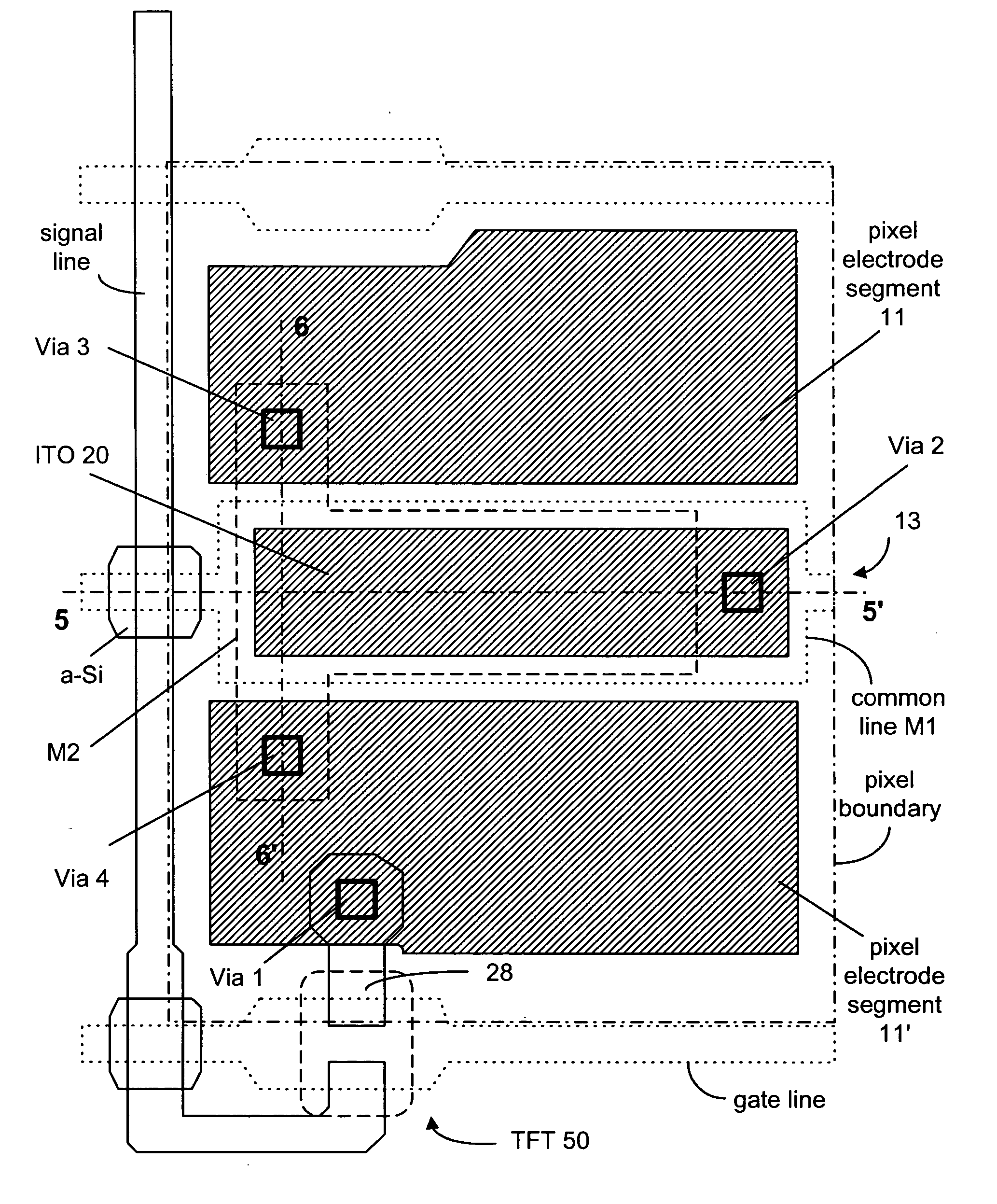
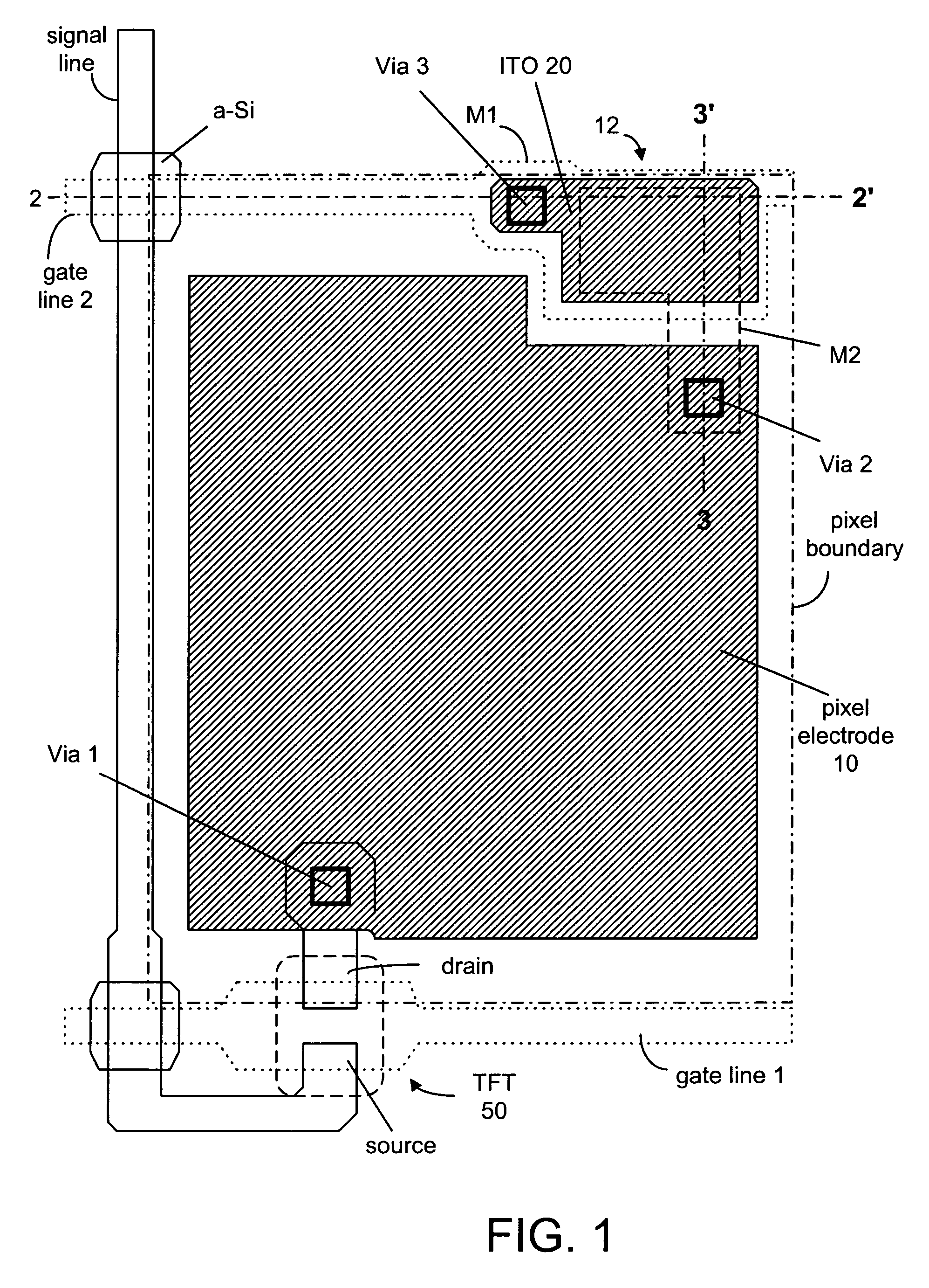
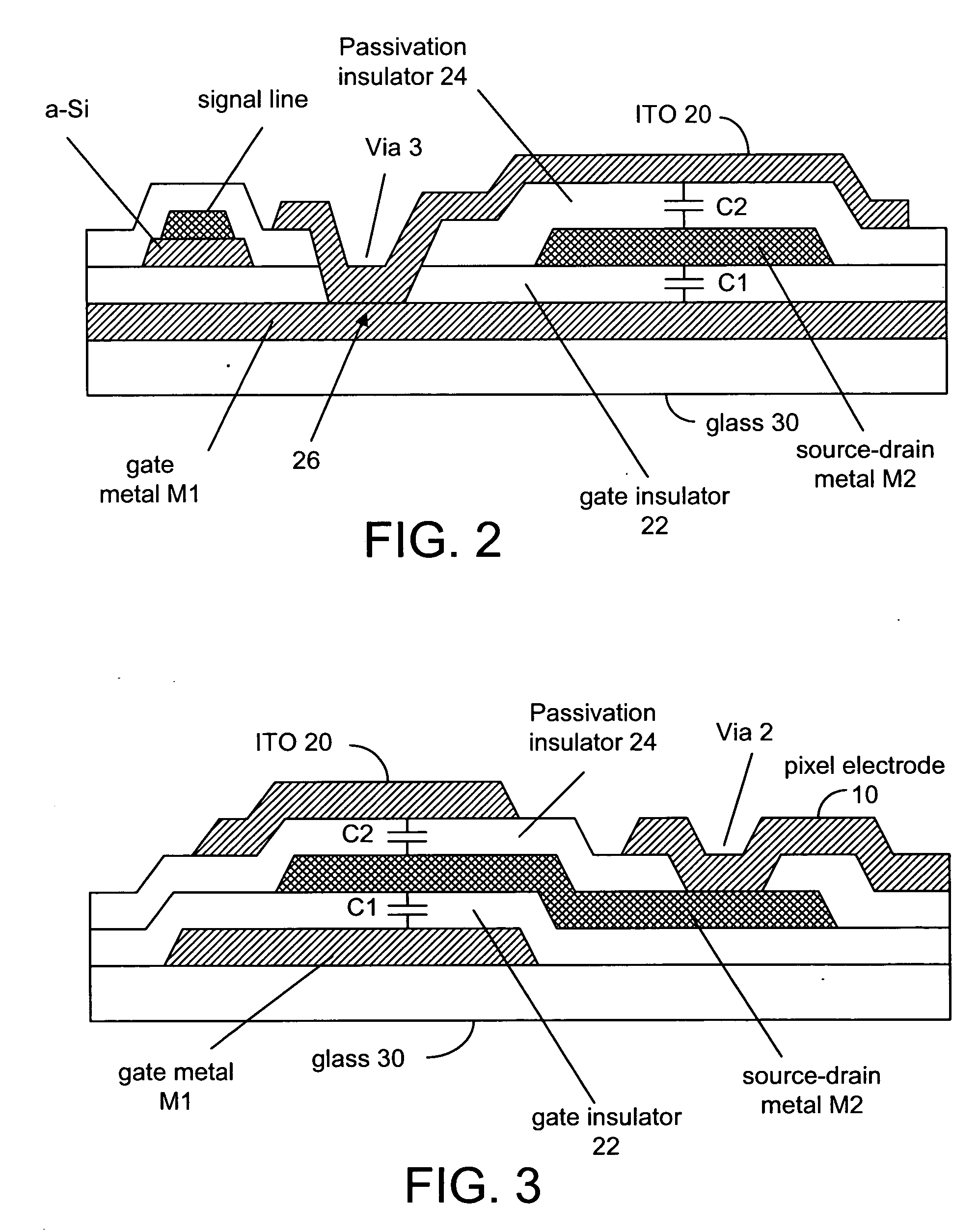
[0053] As best seen in FIGS. 1, 2 and 3, a pixel according to the present invention which typically forms part of a pixel array comprises two general areas, one associated with the pixel electrode 10 and another associated with the control and storage capacitor area 12. The pixel fabrication technique shown in FIGS. 1, 2 and 3 is known in the art as a storage capacitor-on-gate design (Cs-on-gate). The fabrication technique in general is with regard to an amorphous silicon thin film transistor liquid crystal display (a-Si TFT-LCD) although the principles described could be used for other types of TFT-LCD displays, and as a p-Si TFT-LCD display.

[0054] As seen in FIGS. 1, 2 and 3, a storage capacitor for use in maintaining the state of the pixel electrode and thus of the LCD pixel between scans, comprises two storage capacitors shown diagrammatically as C1 and C2. The first capacitor C1 is formed between a first metal layer M1 (gate electrode) and a second metal layer M2. The second c...


PUM


Abstract

A stacked storage capacitor structure for use in each pixel of a TFT-LCD, wherein a first storage capacitor is formed by a first metal layer, a gate insulator layer and a second metal layer. The second capacitor is formed by the second metal layer, a passivation insulator layer and an ITO layer. The first metal layer and the ITO layer are joined together through a via hole which is etched in one insulator etching step during the overall fabrication process through both the gate insulator and the passivation insulator layers. As such, the two capacitors are connected in parallel in a stacked configuration. With the stacked storage capacitor structure, the charge storage capacity is increased without significantly affecting the aperture ratio of a pixel. The ITO and the pixel electrode can be different parts of an indium tine oxide layer deposited on the passivation insulator layer.

Description

TECHNICAL FIELD [0001] The present invention relates to a storage capacitor structure for use in a thin film transistor liquid crystal display particularly an amorphous silicon thin film transistor liquid crystal display. BACKGROUND OF THE INVENTION [0002] It is known in the art that thin film transistor liquid crystal displays (commonly referred to as TFT-LCD) seek to minimize the area needed for the storage capacitor used in such displays especially as the resolution of the display increases and therefore the pixel size decreases. The increase in display resolution is especially important for amorphous silicon TFT-LCD displays (a-Si TFT-LCDs). In particular, it is well known that as the display resolution increases, the area available on each pixel of such displays for the fabrication of the storage capacitor is diminished due to aperture ratio considerations. What this means is that for a given pixel it is desired that as the overall size of the pixel decreases, that the maximum ...

Claims


Application Information

Patent Timeline
IPC IPC(8): G02F1/1343G02F1/133G02F1/136G02F1/1362H01L21/027H01L27/12H01L29/786
CPCG02F1/136213H01L27/12
Inventor LUO, FANG-CHENLO, CHANG-CHENG
Owner AU OPTRONICS CORP
Why Eureka
Try Eureka