Method of manufacturing single crystal Si film

Active Publication Date: 2006-06-08
SAMSUNG ELECTRONICS CO LTD
View PDF11 Cites 50 Cited by
  • Summary
  • Abstract
  • Description
  • Claims
  • Application Information

AI Technical Summary

Benefits of technology

[0017] The dividing layer is located less than 1000 Å below the surface of the S

Problems solved by technology

However, poly crystalline silicon has inferior mobility and homogeneity to single crystal silicon.
A critical factor in manufacturing single crystal silicon is the limitation of temperature.
That is, the manufacturing process can not be performed at a temperature greater than that which the glass or plastic base material can withstand.
The conventional method of manufacturing the SOI wafer limits the use of materials for the substrate and gives a thermal shock to the selected material.
Therefore, obtaining the desired performance from silicon is difficult.

Method used


Image

  • Method of manufacturing single crystal Si film
  • Method of manufacturing single crystal Si film
  • Method of manufacturing single crystal Si film

Examples


Embodiment Construction

[0021] The present invention will now be described more fully with reference to the accompanying drawings in which exemplary embodiments of the invention are shown.

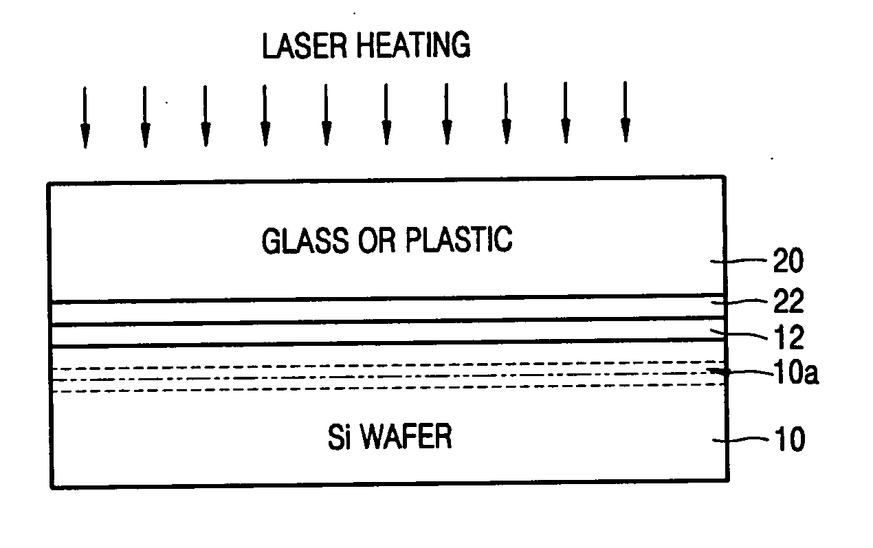
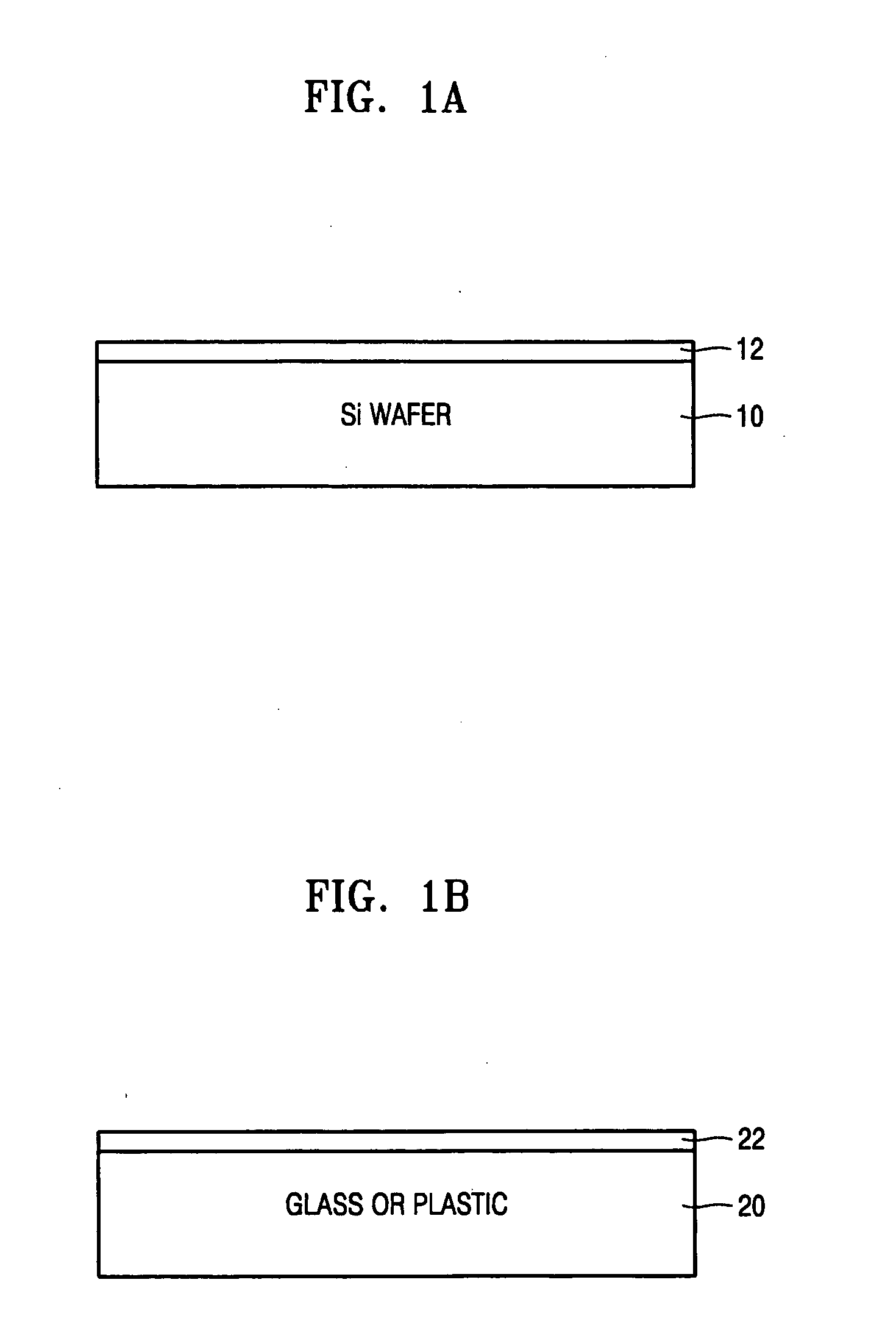
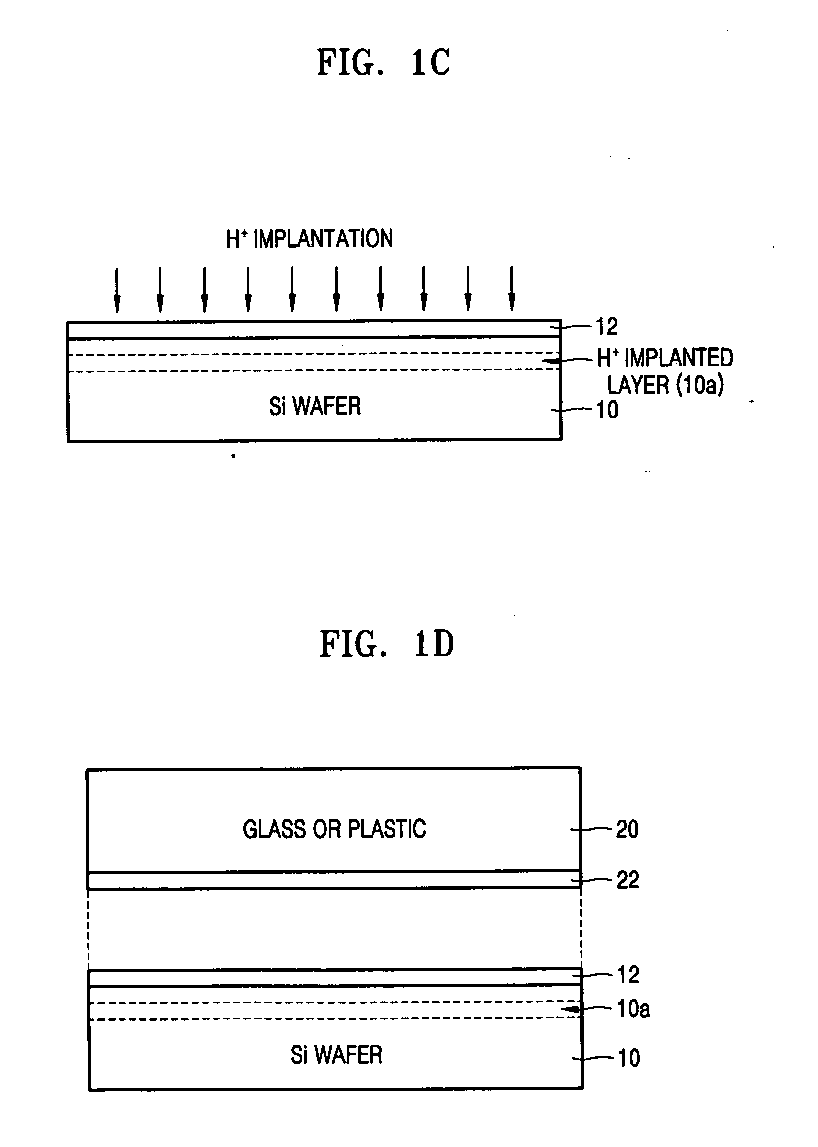
[0022]FIGS. 1A through 1G are cross-sectional views illustrating a method of manufacturing a single crystal Si film according to an embodiment of the present invention.

[0023] Referring to FIGS. 1A and 1B, a first oxide layer 12 is formed on a Si substrate 10, and a second oxide layer 22 is formed on an insulating substrate 20. For example, after preparing the Si substrate 10, the first oxide layer 12, such as a SiO2 layer, can be formed on the Si substrate 10 using chemical vapor deposition (CVD). In the same manner, the second oxide layer 22, such as a SiO2 layer, can be formed on the insulating substrate 20 using CVD. The first oxide layer 12 and the second oxide layer 22 will function as bonding layers, after activation by a surface treatment using oxygen O2 plasma in a subsequent process. A transparent substrate, su...


PUM


Abstract

Provided is a method of manufacturing a single crystal Si film. The method includes: preparing a Si substrate on which a first oxide layer is formed and an insulating substrate on which a second oxide layer is formed; forming a dividing layer at a predetermined depth from a surface of the Si substrate by implanting hydrogen ions from above the first oxide layer; bonding the insulating substrate to the Si substrate so that the first oxide layer contacts the second oxide layer; and forming a single crystal Si film having a predetermined thickness on the insulating substrate by cutting the dividing layer by irradiating a laser beam from above the insulating substrate. Therefore, a single crystal Si film having a predetermined thickness can be formed on an insulating substrate.

Description

CROSS-REFERENCE TO RELATED PATENT APPLICATIONS [0001] This application claims the benefit of Korean Patent Application No. 10-2004-00101118, filed on Dec. 3, 2004, in the Korean Intellectual Property Office, the disclosure of which is incorporated herein in its entirety by reference. BACKGROUND OF THE INVENTION [0002] 1. Field of the Invention [0003] The present invention relates to a method of manufacturing a single crystal Si film, and more particularly, to a method of manufacturing a single crystal Si film that can be formed on a substrate which is sensitive to heat. [0004] 2. Description of the Related Art [0005] Poly crystalline silicon (poly-Si) is applied to various electronic devices, such as flat display devices and solar cells, due to its high mobility compared to amorphous silicon (a-Si). However, poly crystalline silicon has inferior mobility and homogeneity to single crystal silicon. [0006] Single crystal silicon is especially useful in a system on panel (SOP) structure...

Claims


Application Information

Patent Timeline
IPC IPC(8): H01L21/30
CPCH01L21/76254H01L27/12
Inventor NOGUCHI, TAKASHIXIANYU, WENXUYIN, HUAXIANG
Owner SAMSUNG ELECTRONICS CO LTD
Why Eureka
Try Eureka