

Semiconductor substrate, manufacturing method thereof, and semiconductor device
a technology of semiconductor devices and semiconductor substrates, applied in the direction of semiconductor/solid-state device manufacturing, semiconductor devices, electrical devices, etc., can solve the problems of different dopant diffusion, ge diffusion, metal contact formation, etc., and achieve the same problems in the structure having an insulating layer
- Summary
- Abstract
- Description
- Claims
- Application Information
AI Technical Summary
Benefits of technology
Problems solved by technology
Method used
Image

Examples
first embodiment
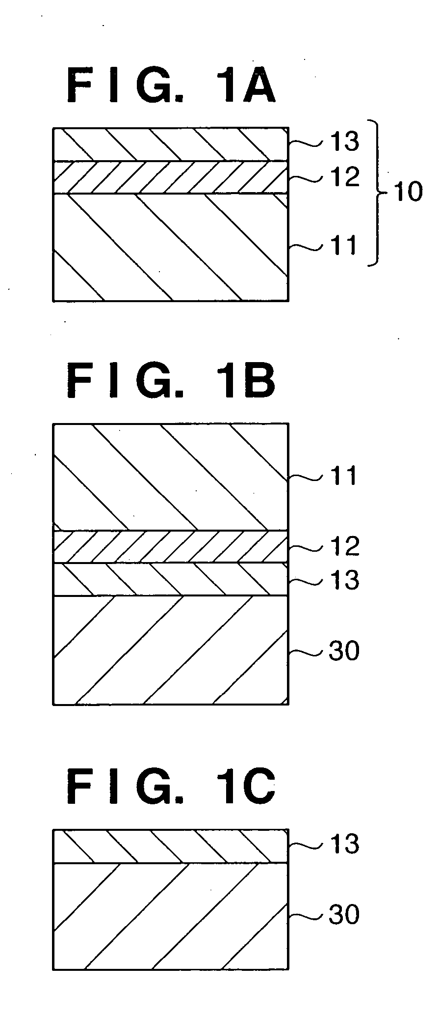
[0024] A strain induction layer is formed on the surface of a semiconductor substrate made of a second material. A strained semiconductor layer made of a first material is formed on the strain induction layer to prepare a first substrate. A second substrate made of a first material is bonded to the first substrate. The semiconductor substrate made of the second material and the strain induction layer are removed. Accordingly, the strained semiconductor layer made of the first material can be formed on the second substrate made of the first material while being in contact with the second substrate.
[0025] As the first and second materials, silicon is typically used.
[0026] As the strain induction layer, a layer (Si1-xGex layer) containing silicon and germanium is formed. A layer (preferably, a single-crystal silicon layer) almost made of silicon is formed on the Si1-xGex layer as a strained semiconductor layer.
[0027] In the Si1-xGex layer formed on the semiconductor substrate made o...
second embodiment
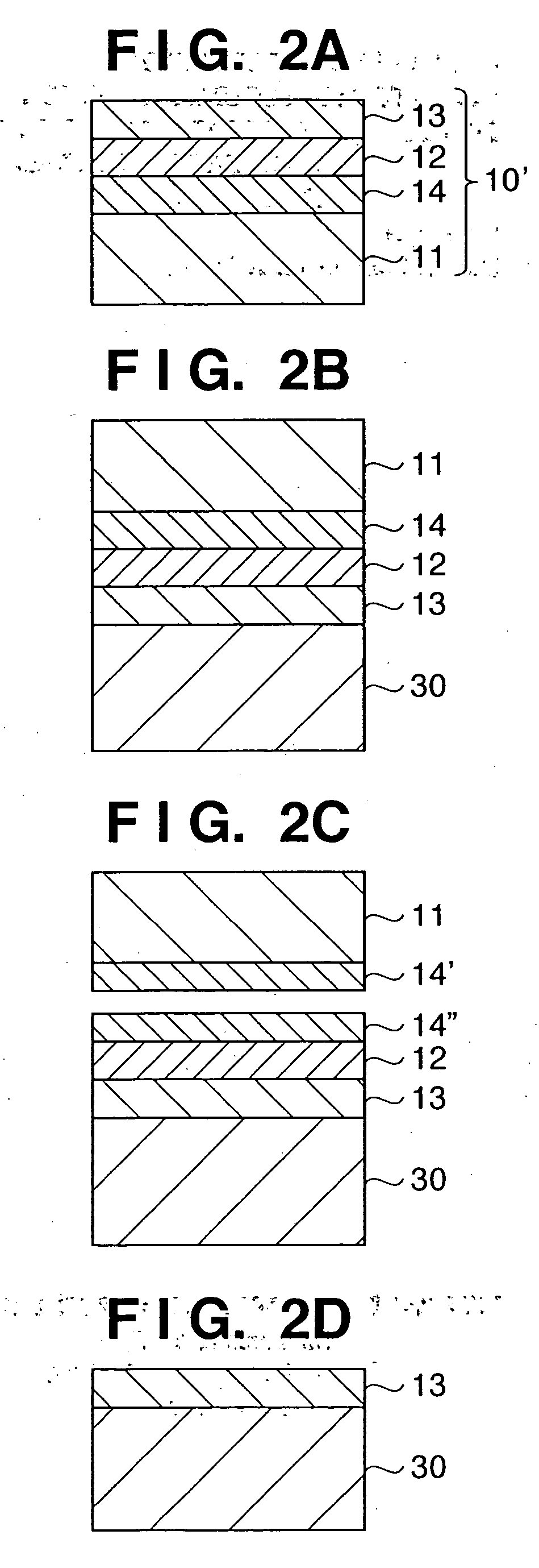
[0031] A separation layer is formed on the surface of a semiconductor substrate made of a second material. A strain induction layer is formed on the separation layer. In addition, a strained semiconductor layer made of a first material is formed on the strain induction layer to prepare a first substrate.
[0032] A second substrate made of a first material is bonded to the first substrate. The members are separated at the separation layer. After that, the remaining separation layer and strain induction layer are removed. Accordingly, the strained semiconductor layer made of the first material can be formed on the second substrate made of the first material while being in contact with the second substrate.
[0033] As the first and second materials, silicon is typically used. The separation layer can be formed typically by porosifying the surface of the semiconductor substrate (silicon substrate) made of the second material by anodizing. As another method, after the strain induction laye...
third embodiment
[0040] A separation layer is formed on the surface of a semiconductor substrate made of a second material. A strain induction layer is formed on the separation layer. In addition, a strained semiconductor layer made of a first material is formed on the strain induction layer to prepare a first substrate.
[0041] A second substrate made of a first material is bonded to the first substrate. The members are separated at the separation layer. After that, the remaining separation layer and strain induction layer are removed. Accordingly, the strained semiconductor layer made of the first material can be formed on the second substrate made of the first material while being in contact with the second substrate.
[0042] As the first and second materials, silicon is typically used.
[0043] The separation layer can be formed typically by porosifying the surface of the semiconductor substrate (silicon substrate) made of the second material by anodizing.
[0044] As the strain induction layer, a lay...
PUM
 Abstract
Description
Claims
Application Information