Microlens array sheet and method for manufacturing the same

a technology of microlens array and microlens, which is applied in the direction of filtration separation, instruments, separation processes, etc., can solve the problems of increasing production costs and time, increasing the manufacturing price of products, and difficulty in rapid development of new products, so as to achieve no optical loss and improve optical efficiency

Inactive Publication Date: 2006-06-15
LG ELECTRONICS INC
View PDF3 Cites 19 Cited by
  • Summary
  • Abstract
  • Description
  • Claims
  • Application Information

AI Technical Summary

Benefits of technology

[0010] Therefore, the present invention has been made in view of the above problems, and it is an object of the present invention to provide a microlens array sheet and a method for manufacturing the same, wherein no optical loss is generated when the microlens array sheet is manufactured, whereby an improved optical efficiency can be accomplished and a viewing angle of microlenses can be controlled.

Problems solved by technology

This inevitably results in an increase in production costs and time.
For this reason, when devices, having short development period and product life, are manufactured via the sequential semiconductor processes, there exist problems, for example, an increase in the manufacturing price of products, and a difficulty in the rapid development of new products.
Furthermore, when a pattern is manufactured via a photo-exposure process, it is difficult to achieve a micro pattern less than a predetermined level due to a limit of an optical source.
However, in the case of patterns manufactured by the laser micro machining, the boundary region of the patterns cannot have a vertical cross section.
This is due to optical loss in the boundary region of the patterns when the patterns are applied to an optical sheet of a display system.

Method used


Image

  • Microlens array sheet and method for manufacturing the same
  • Microlens array sheet and method for manufacturing the same
  • Microlens array sheet and method for manufacturing the same

Examples


Embodiment Construction

[0021] Now, a preferred embodiment of the present invention will be explained with reference to the accompanying drawing. In the following description, a detailed description of known functions and configurations incorporated herein will be omitted when it may make the subject matter of the present invention rather unclear.

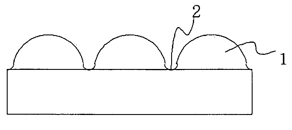
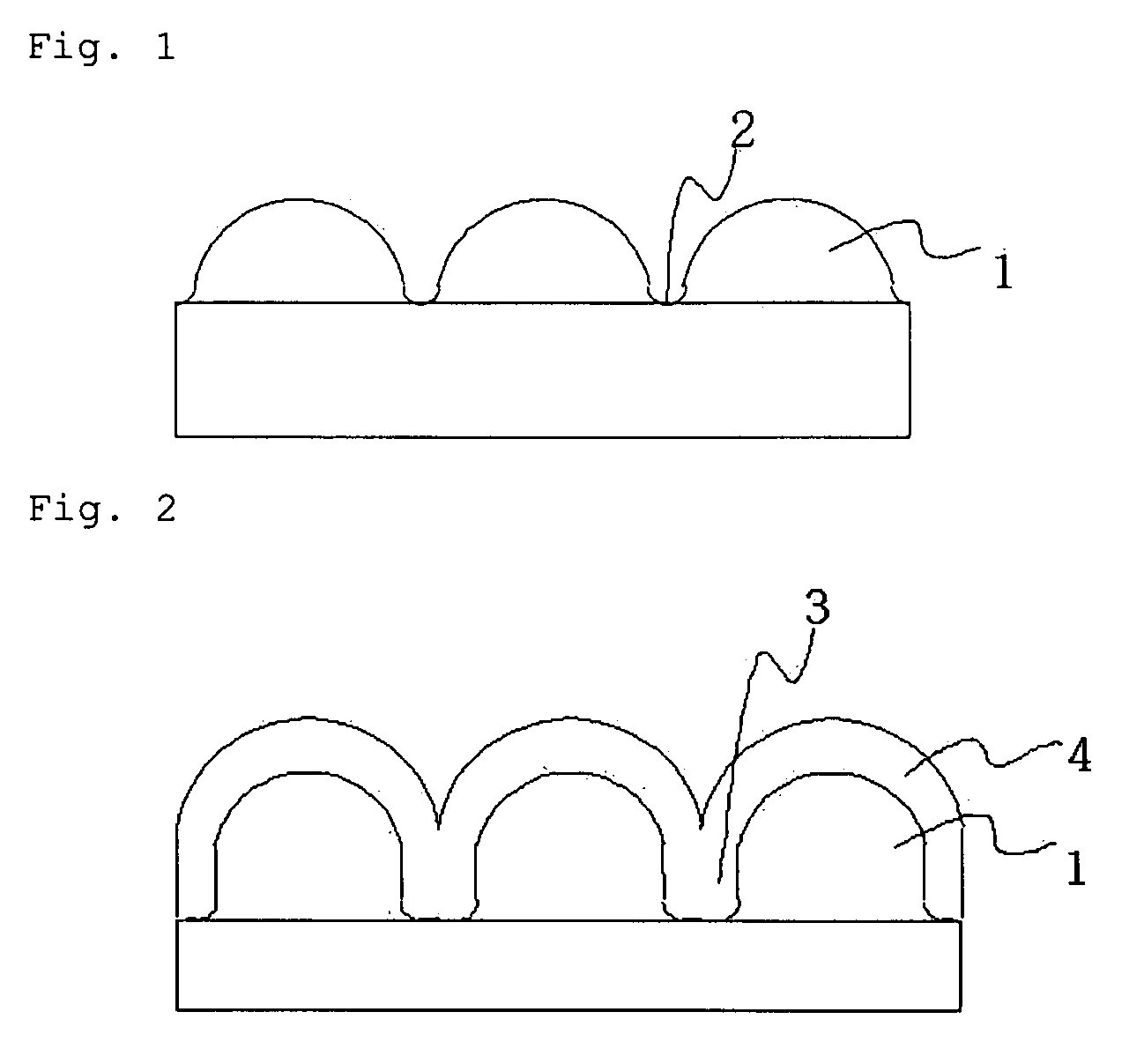
[0022]FIG. 2 is a sectional view of a microlens array sheet using micro machining according to an embodiment of the present invention.

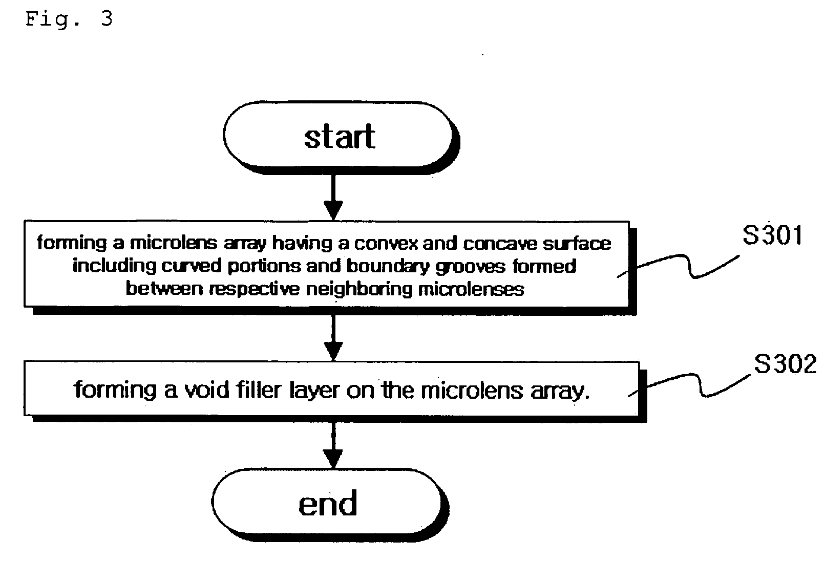
[0023] In the embodiment of the present invention, the microlens array sheet includes a microlens array 1, and a void filler layer 4.

[0024] The embodiment of the present invention schematically exemplifies a method for forming one or more boundary grooves 3 in the microlens array 1.

[0025] Referring to FIG. 2, the boundary grooves 3 are formed in the microlens array 1 in a laser micro machining step of the microlens array 1, in order to minimize optical loss in the boundary regions between respective neighboring microlenses, whic...


PUM

PropertyMeasurementUnit
light emitting angleaaaaaaaaaa
sizeaaaaaaaaaa

Abstract

Disclosed herein are a microlens array sheet using micro machining and a method for manufacturing the same. The microlens array sheet comprises a microlens array having a convex and concave surface including curved portions and boundary grooves formed between respective neighboring microlenses via laser micro machining, and a void filler layer stacked on the microlens array. The microlens array sheet can be manufactured with a reduced number of process steps using laser micro machining, whereby improved productivity as compared to a conventional sequential semiconductor process can be accomplished. Using the laser micro machining, also, enables the manufacture of a desired three-dimensional micro shape. Therefore, the microlens array sheet is applicable as an optical sheet of a display system requiring a delicate surface shape.

Description

[0001] This application claims the benefit of the Korean Patent Application No. 10-2004-0105873, filed on Dec. 14, 2004, which is hereby incorporated by reference as if fully set forth herein. BACKGROUND OF THE INVENTION [0002] 1. Field of the Invention [0003] The present invention relates to a microlens array sheet and a method for manufacturing the same. [0004] 2. Description of the Related Art [0005] As well known, laser micro machining has several advantages in that it can manufacture complicated three-dimensional structures in a more simplified manner as compared with using conventional semiconductor processing, and that it requires relatively simple equipment. Therefore, laser micro machining has attracted a lot of attention. Moreover, the laser micro machining can process various materials, such as for example, ceramics, metals, and polymers, in addition to semiconductor materials. [0006] A representative example of three-dimensional structure manufacturing methods using lase...

Claims


Application Information

Patent Timeline
Patent Type & Authority Applications(United States)
IPC IPC(8): G02B27/10B81B1/00B81C99/00G02B3/00G03B21/62G03B21/625
CPCB29D11/00278G02B3/0025G02B3/0031G02B3/005G02B3/0056
Inventor OH, CHANG-HOONKWON, HYOUKLIM, TAE-SUNYEE, YOUNG-JOOPARK, KI-WONSEONG, DONG-MUGLEE, GUN-WOON
Owner LG ELECTRONICS INC
Why Eureka
Try Eureka