Semiconductor laser apparatus capable of routing laser beams emitted from stacked-array laser diode to optical fiber with little loss

a laser apparatus and semiconductor technology, applied in semiconductor lasers, instruments, optical elements, etc., can solve the problem of not easily achieving the high power density that is a feature of laser processing

Active Publication Date: 2006-06-15
NIPPON STEEL CORP
View PDF2 Cites 70 Cited by
  • Summary
  • Abstract
  • Description
  • Claims
  • Application Information

AI Technical Summary

Benefits of technology

[0009] One of the objects of the present invention is to provide a semiconductor laser apparatus capable of routing laser beams emitted from a stacked-array laser diode to an optical fiber with a little loss.

Problems solved by technology

A high power density that is a feature of laser processing is not attained readily.

Method used


Image

  • Semiconductor laser apparatus capable of routing laser beams emitted from stacked-array laser diode to optical fiber with little loss
  • Semiconductor laser apparatus capable of routing laser beams emitted from stacked-array laser diode to optical fiber with little loss
  • Semiconductor laser apparatus capable of routing laser beams emitted from stacked-array laser diode to optical fiber with little loss

Examples


Embodiment Construction

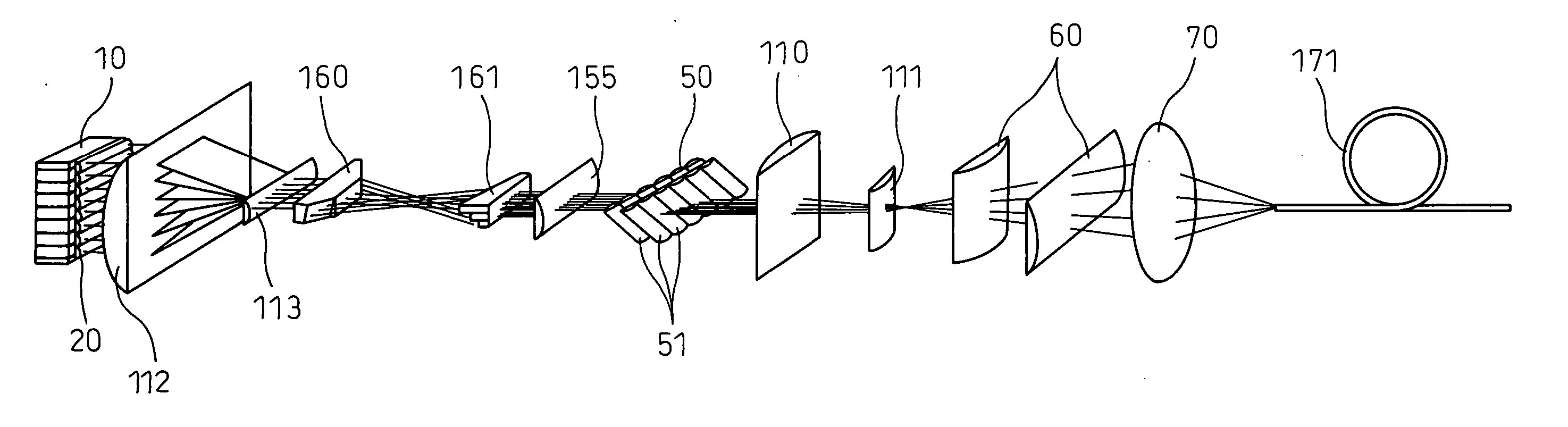
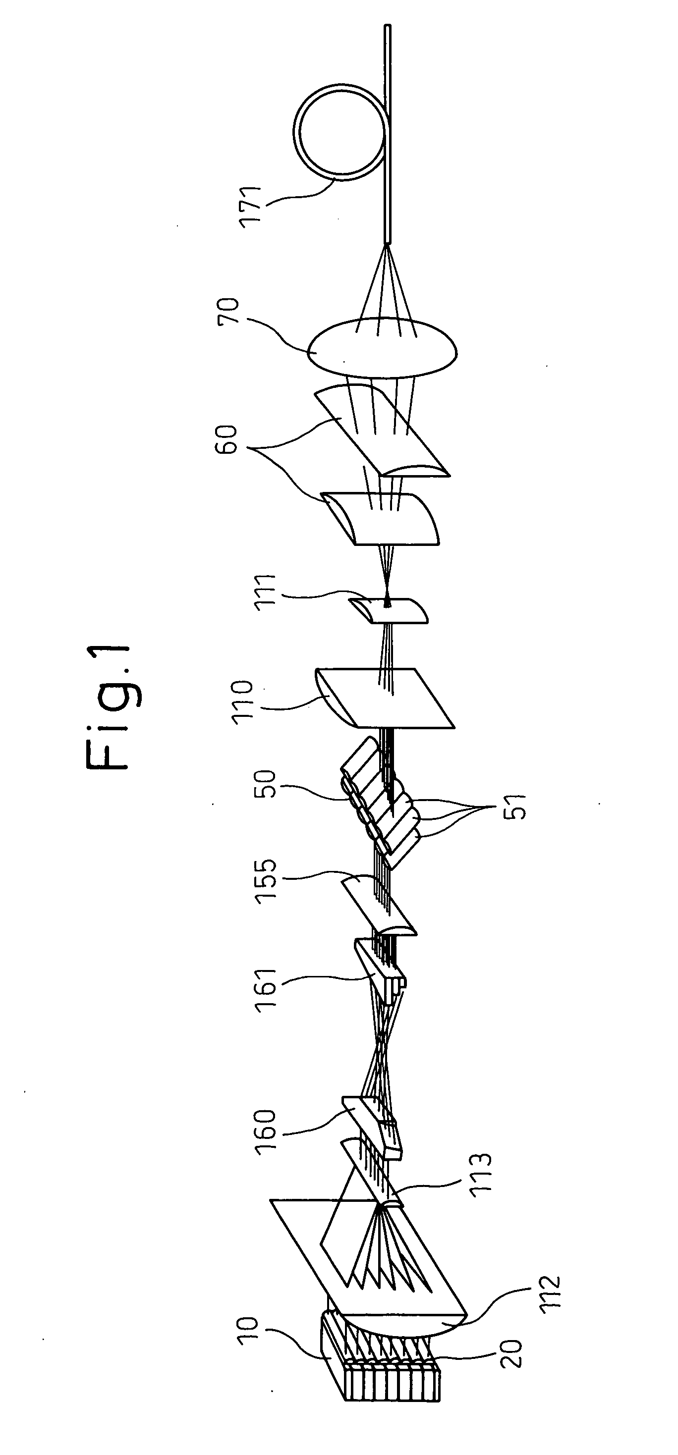
[0043] For the purposes of the discussion provided herein below, with respect to one exemplary embodiment of the present invention, a position in front of an optical device can signify a position on the side of a point at which the optical device converges light, and a position behind the optical device signifies a position on the side of a light source (opposite to the position in front of the optical device). Moreover, the same reference numerals as those employed in description of exemplary embodiments of the present invention will be used throughout this document. In the specification and drawings, the same reference numerals will be assigned to components having substantially the same functions. It should be noted that the reference numerals are used merely for a further understanding, and in no way meant to, in any way, restrict the present invention to those described herein.

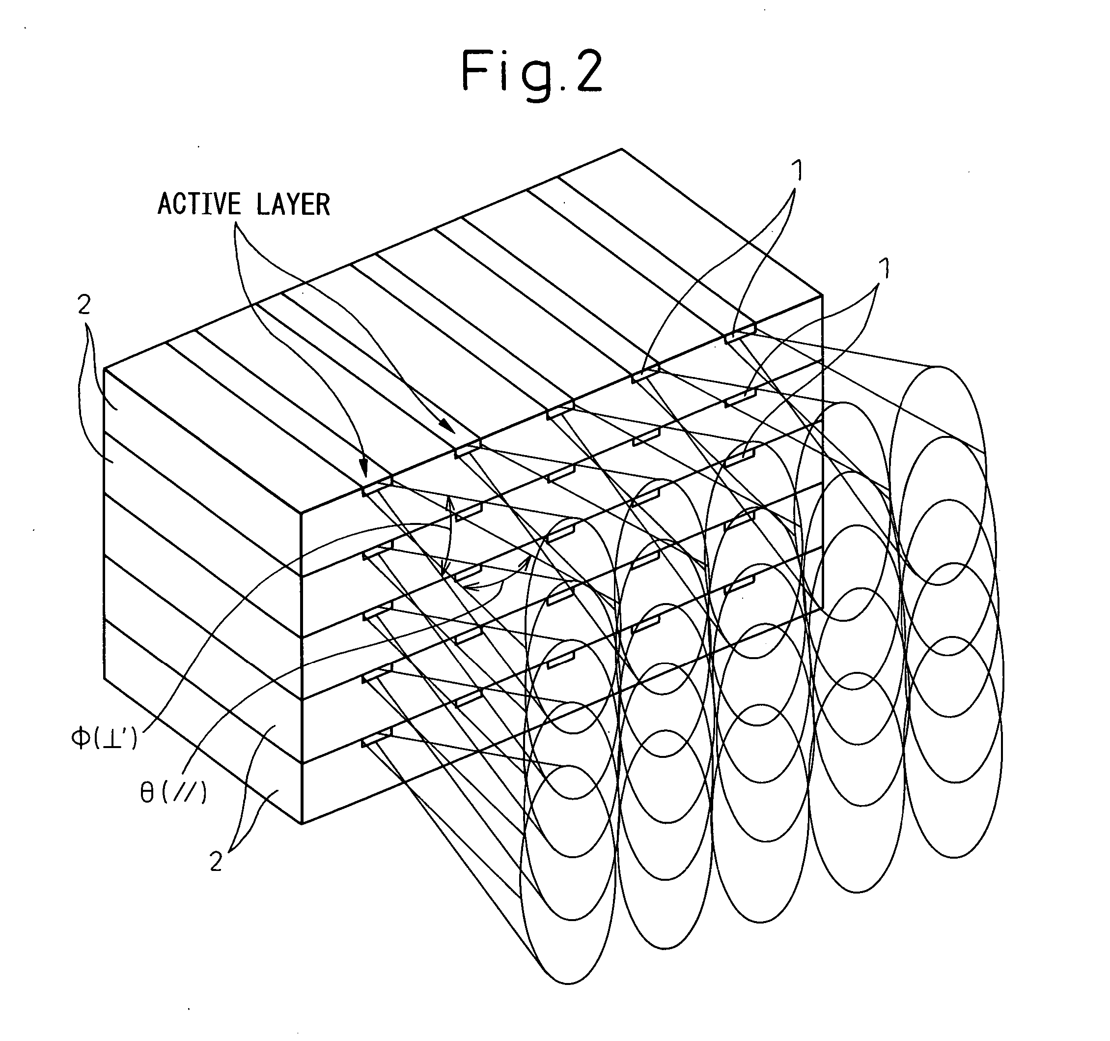
[0044] Prior to describing exemplary embodiments of the present invention, a conventional semiconduct...


PUM


Abstract

A semiconductor laser apparatus according to an exemplary embodiment of the present invention is provided. For example, the apparatus may include a single or a plurality of stacked-array laser diodes, first beam compressors, and a separating optical device separating the group of laser beams into subgroups of laser beams in a first direction, and deflecting the subgroups of laser beams so that the subgroups of laser beams approach in the first direction and recede from one another in a second direction. In addition, a collimating optical device may be provided which is adapted to deflect the subgroups of laser beams in the first and second directions by the same angles. Further, a beam converter may be included which divides each subgroup of laser beams and turning the axis thereof, and second beam compressors and a group of cylindrical lenses can be provided that can make the angle of divergence in the first direction close to the angle of divergence in the second direction.

Description

CROSS-REFERENCE TO RELATED APPLICATION(S) [0001] This application is based upon and claims the benefit of priority from the prior Japanese Patent Application No. 2004-363600, filed on Dec. 15, 2004, the entire disclosure of which is incorporated herein by reference. FIELD OF THE INVENTION [0002] The present invention relates to a semiconductor laser apparatus, and more particularly, to the semiconductor laser apparatus that uses a beam conversion optical system to converge a group of laser beams radiated from a stacked-array laser diode, and routes the resultant group of laser beam to an optical fiber. BACKGROUND INFORMATION [0003] In recent years, a linear-array semiconductor laser having stripes of active layers formed one-dimensionally has been available in a continuous-wave oscillation type providing a power output of about 50 W. The linear-array semiconductor laser has stripes, which has a width ranging from 100 μm to 200 μm and has one ends thereof formed as emitters, equidist...

Claims


Application Information

Patent Timeline
Patent Type & Authority Applications(United States)
IPC IPC(8): H01S5/00
CPCG02B6/425G02B27/0961G02B27/0966G02B27/0972H01S5/005H01S5/02284H01S5/4012H01S5/405G02B19/0057G02B19/0028G02B19/0014H01S5/02251
Inventor KIDO, MOTOIIMAI, HIROFUMIHAMADA, NAOYA
Owner NIPPON STEEL CORP
Why Eureka
Try Eureka