White organic electroluminescent device
a technology of electroluminescent devices and white organic materials, which is applied in the direction of discharge tube luminescnet screens, natural mineral layered products, transportation and packaging, etc., can solve the problems of insufficient efficiency of this device at a brightness of 200 cd/m, insufficient control of the same in a large-scale production process, etc., and achieves high efficiency and high brightness. , the effect of high lifetim
- Summary
- Abstract
- Description
- Claims
- Application Information
AI Technical Summary
Benefits of technology
Problems solved by technology
Method used
Image
Examples
embodiment 1
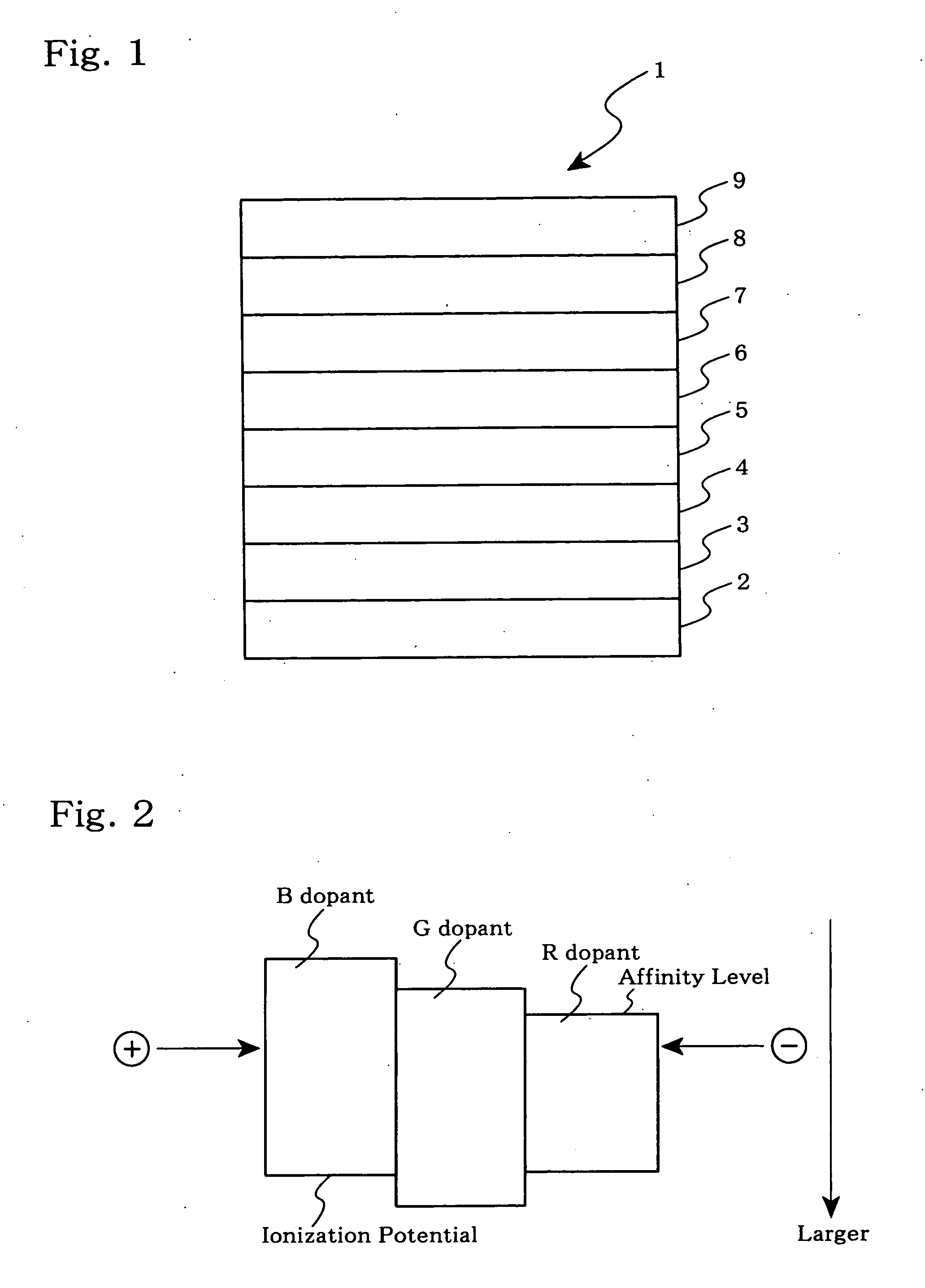
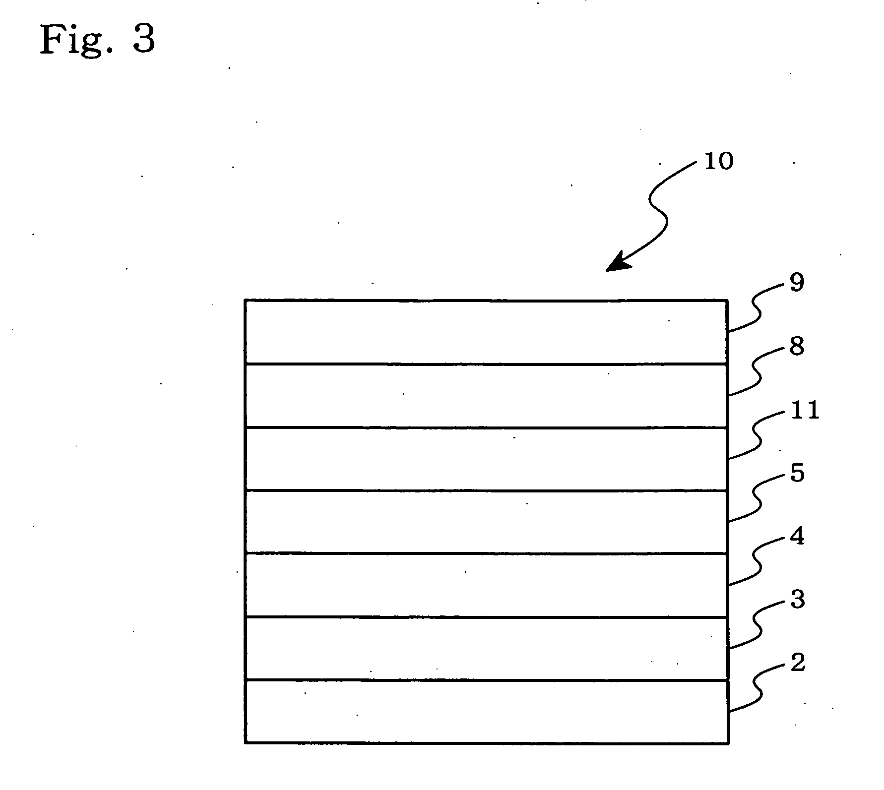
[0046]FIG. 1 is a diagram showing the constitution of a white organic EL device according to one embodiment of the invention. FIG. 2 is an energy level diagram of a blue (B) dopant, a green (G) dopant and a red (R) dopant which form a blue emitting layer, a green emitting layer and a red emitting layer, respectively, in the above white organic EL device.
[0047] As shown in FIG. 1, the white organic EL device 1 has a structure in which an anode 2, a hole injecting layer 3, a hole transporting layer 4, a blue emitting layer 5, a green emitting layer 6, a red emitting layer 7, an electron transporting layer 8 and a cathode 9 are stacked.
[0048] The blue emitting layer 5 contains a host material and a blue dopant, the green emitting layer 6 contains a host material and a green dopant that is an aromatic amine compound of the following formula (1), and the red emitting layer 7 contains a host material and a red dopant.
[0049]FIG. 2 shows energy levels of the blue (B) dopant, the green (G...
embodiment 2
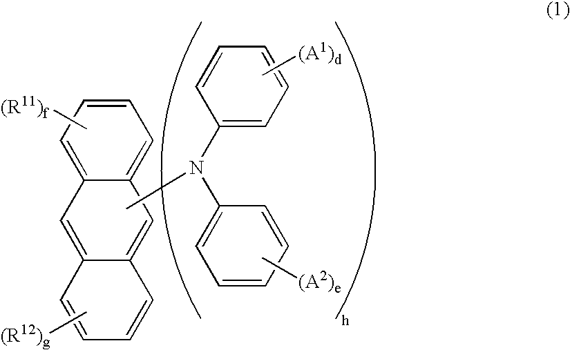
[0062]FIG. 3 is a diagram showing the constitution of a white organic EL device according to another embodiment of the invention. As shown in this Figure, a white organic EL device 10 has a structure in which an anode 2, a hole injecting layer 3, a hole transporting layer 4, a blue emitting layer 5, a green / red emitting layer 11, an electron transporting layer 8 and a cathode 9 are stacked. That is, the white organic EL device 10 of this embodiment differs from the white organic EL device 1 of embodiment 1 in that the green / red emitting layer 11 is provided in place of the green emitting layer 6 and the red emitting layer 7.
[0063] The blue emitting layer 5 contains a host material and a blue dopant, and the green / red emitting layer 11 contains a host material, a green dopant that is an aromatic amine compound of the following formula (1) and a red dopant.
[0064] In the white organic EL device 10 of this embodiment, the blue emitting layer 5 and the green / red emitting layer 11 are s...
examples
[0202] Examples of the invention will be described below, but the invention is not limited to these examples.
PUM
| Property | Measurement | Unit |
|---|---|---|
| ionization potential | aaaaa | aaaaa |
| maximum wavelength | aaaaa | aaaaa |
| thickness | aaaaa | aaaaa |
Abstract
Description
Claims
Application Information
 - R&D
- Intellectual Property
- Life Sciences
- Materials
- Tech Scout
- Unparalleled Data Quality
- Higher Quality Content
- 60% Fewer Hallucinations
Browse by: Latest US Patents, China's latest patents, Technical Efficacy Thesaurus, Application Domain, Technology Topic, Popular Technical Reports.
© 2025 PatSnap. All rights reserved.Legal|Privacy policy|Modern Slavery Act Transparency Statement|Sitemap|About US| Contact US: help@patsnap.com


