Process for producing negative charging electrophotographic photosensive member, negative charging electrophotographic photosensitive member, and electrophotographic apparatus using same

a technology of electrophotographic photosensitive and electrophotographic photosensitive parts, which is applied in the direction of electrographic process apparatus, optics, instruments, etc., can solve the problems of low mutual adhesion between layers, achieve the effect of improving adhesion, reducing image defects, and simplifying film forming steps

Inactive Publication Date: 2006-06-15
CANON KK
View PDF6 Cites 1 Cited by
  • Summary
  • Abstract
  • Description
  • Claims
  • Application Information

AI Technical Summary

Benefits of technology

[0032] As described above, according to the negative-charging electrophotographic photosensitive member production process of the present invention, it has the step of plasma treatment which forms an interface having the ability of blocking the acquired electric charges, at the surfaces of the protuberances at least the vertexes of which have been removed, thereby making it unnecessary to deposit an upper-part blocking layer as a second layer and achieving the improvement of the adherence between layers while maintaining the effect of lessening image defects. The simplification of film forming steps is also concurrently achieved to realize a reduction in overall costs. Also, inasmuch as the compositional ratio of carbon to silicon which constitute the upper-part blocking layer deposited as the first layer increases toward the surface side, potential non-uniformity can be controlled.

Problems solved by technology

Accordingly, where, as conventionally done, a photosensitive member is set again in a film forming furnace after the polishing is carried out to flatten the protuberances and then the upper-part blocking layer is deposited as a second layer, a problem may arise such that the low mutual adherence between layers may result.
This problem is caused by the layer configuration in which, where a protective layer deposited for the purpose of preventing the photosensitive member from being scratched by the polishing and the upper-part blocking layer are formed as layers formed of a non-single-crystal material containing at least carbon and silicon, an upper-part blocking layer having a relatively low carbon content is deposited after a protective layer having a relatively high carbon content has been deposited.

Method used


Image

  • Process for producing negative charging electrophotographic photosensive member, negative charging electrophotographic photosensitive member, and electrophotographic apparatus using same
  • Process for producing negative charging electrophotographic photosensive member, negative charging electrophotographic photosensitive member, and electrophotographic apparatus using same
  • Process for producing negative charging electrophotographic photosensive member, negative charging electrophotographic photosensitive member, and electrophotographic apparatus using same

Examples


example 1

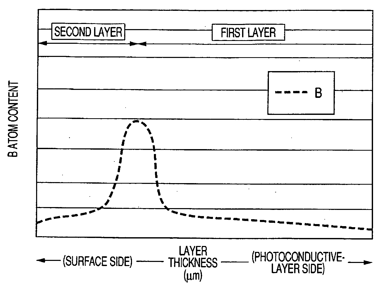
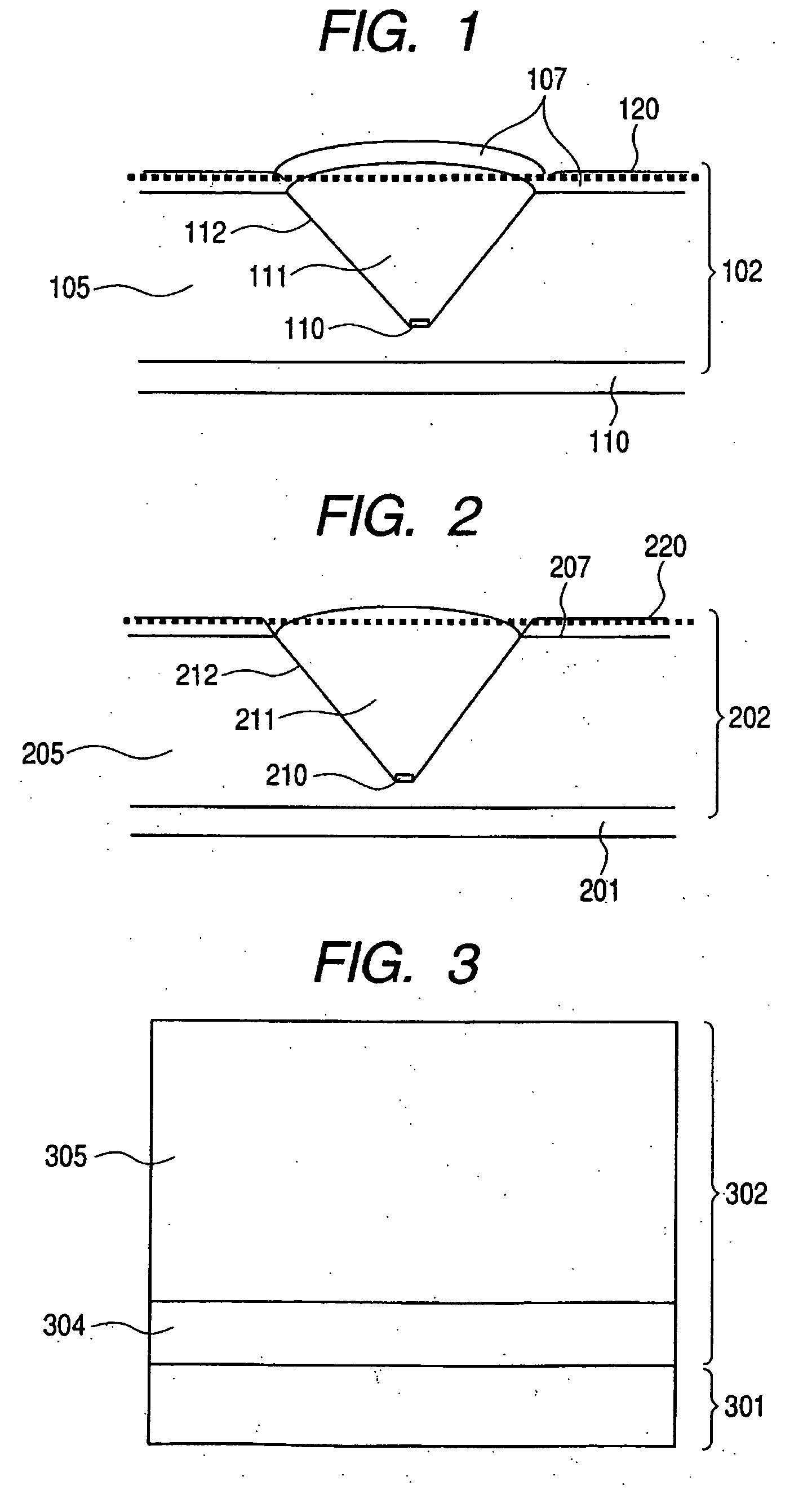
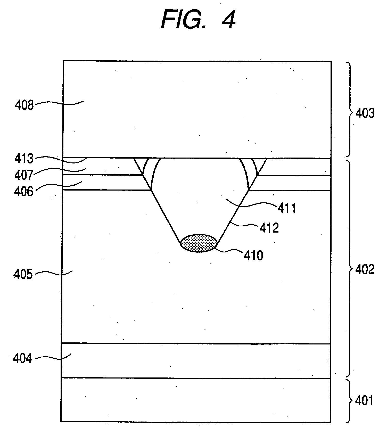
[0135] Using the a-Si photosensitive member film forming apparatus shown in FIG. 5, which is of an RF plasma-assisted CVD system, a lower-part blocking layer formed of at least a non-single-crystal material and a photoconductive layer formed of at least a non-single-crystal material were deposited as the first layer on an aluminum substrate of 80 mm in outer diameter under conditions shown in Table 1. Thereafter, the substrate with the first layer deposited thereon was taken out of the film forming furnace to expose it to the atmosphere, and thereafter subjected to polishing to remove protuberances at least at their vertexes on the first layer surface, and then to the treatment of bringing the first layer surface into contact with water. Thereafter, the substrate with the first layer deposited thereon, which had been processes in this way, was placed in the film forming furnace, and, before the second layer was deposited, subjected to plasma treatment in which, as to the boron conte...

example 2

[0144] According to the procedure of Example 1, which was changed only in that the treatment of bringing the first layer surface into contact with water was not carried out, a negative-charging electrophotographic photosensitive member was produced under conditions shown in Table 5. In respect of costs, the adherence between layers, polishing mars, chargeability, image defects and potential non-uniformity, evaluation was made in the manner as described below. Results obtained are shown in Table 18.

example 3

[0145] According to the procedure of Example 1, which was changed only in that in the first layer, the upper-part blocking layer formed of at least a non-single-crystal material was additionally deposited, a negative-charging electrophotographic photosensitive member was produced under conditions shown in Table 6. In respect of costs, the adherence between layers, polishing mars, chargeability, image defects and potential non-uniformity, evaluation was made in the manner as described below. Results obtained are shown in Table 18.


PUM


Abstract

The invention provides a process for producing a negative-charging electrophotographic photosensitive member which can improve the adherence between a first layer and a second layer without lowering the effect of lessening image defects and realize a reduction in overall costs, a negative-charging electrophotographic photosensitive member produced by the process, and an electrophotographic apparatus. In the process for producing a negative-charging electrophotographic photosensitive member, a first layer is deposited on a substarte, at least the vertexes of protuberances are removed, the substrate with the first layer deposited theron is placed in a film forming furnace, the first layer surface is plasma-treated with a gas containing at least a Group 13 element in the periodic table and a dilution gas composed of at least one selected from hydrogen, argon and helium, and a layer formed of a non-single-crystal material is deposited as the second layer on the first layer.

Description

[0001] This application is a continuation of International Application No. PCT / JP2005 / 015387, filed Aug. 18, 2005, which claims the benefit of Japanese Patent Applications No. 2004-239490, filed Aug. 19, 2004 and No. 2005-227750, filed Aug. 5, 2005.BACKGROUND OF THE INVENTION [0002] 1. Field of the Invention [0003] This invention relates to a process for producing a negative-charging electrophotographic photosensitive member which can reduce image defects and maintain good image formation over a long period of time, and also relates to a negative-charging electrophotographic photosensitive member and an electrophotographic apparatus. [0004] 2. Relared Background Art [0005] Materials that form photoconductive layers in solid-state image pick-up devices or in electrophotographic photosensitive members in the field of image formation or in character readers are required to have properties as follows: They are highly sensitive, have a high SN ratio [photocurrent (Ip) / dark current (Id)],...

Claims


Application Information

Patent Timeline
Patent Type & Authority Applications(United States)
IPC IPC(8): G03G5/14
CPCG03G5/005G03G5/08228G03G5/14704G03G5/08278G03G5/08257
Inventor OHIRA, JUNKOJIMA, SATOSHIAOKI, MAKOTOHOSOI, KAZUTO
Owner CANON KK
Why Eureka
Try Eureka