Non-contact discrete removal of substrate surface contaminants/coatings, and method, apparatus, and system for implementing the same

a non-contact, discrete technology, applied in the direction of laser beam welding apparatus, manufacturing tools, welding/soldering/cutting articles, etc., can solve the problems of difficult control of photoablation process nature, detrimental effect on integrated circuit device performance, and difficult management of thermal processes

Inactive Publication Date: 2006-06-22
LAM RES CORP
View PDF7 Cites 9 Cited by
  • Summary
  • Abstract
  • Description
  • Claims
  • Application Information

AI Technical Summary

Benefits of technology

[0017] Other aspects and advantages of the invention will become apparent from the following detailed description, taken in conjunction with the accompanying drawings, illustrating by way of example the principles of the invention.

Problems solved by technology

Failure to remove a desired layer or the particulate contaminants from wafer surfaces can have detrimental effects on the performance of integrated circuit devices.
Several drawbacks can be associated with using the energy generated in the conventional laser cleaning systems.
One of such limitations is the fairly difficult to control nature of the photoablation processes.
However, because thermal processes are hard to manage, the wafer surface defined directly underneath the location of the removed particulate contaminants / film / coating can be damaged.
Additionally, the rather hard to control nature of the thermal processes can further damage the edges of the remaining film / coating surrounding the locally detached and removed portions.
As such, thermal processes can be unsuitable for precise and discrete removal of the particulate contaminants or portions of films / coatings.
Yet another limitation associated with the conventional laser cleaning systems is the rather narrow range of UV light beam intensities (i.e., energy) supported by the typical laser systems suitable for removal of the particulate contaminants / films / coatings from the wafer surface.
However, again, implementing high intensity UV light beams can damage the wafer surface defined directly underneath the location of the detached particulate contaminant or the removed portion of film or coating.
Still another limitation is that the conventional laser systems are used in conjunction with custom gas recipes.
However, to achieve effective cleaning, complicated and expensive gas recipes should be obtained and implemented.
However, although the silicon oxide film has been damaged so some extent, the silicon oxide film has remained intact.
As can be seen, the silicon surface defined directly underneath the removed portion of the silicon oxide film has been damaged.
Accordingly, the nanosecond conventional laser cleaning systems can damage wafer surfaces being prepared.
Such damages are disfavored as the condition of the wafer surfaces and the operation of the wafers can be adversely affected, ultimately lowering the process yield.

Method used


Image

  • Non-contact discrete removal of substrate surface contaminants/coatings, and method, apparatus, and system for implementing the same
  • Non-contact discrete removal of substrate surface contaminants/coatings, and method, apparatus, and system for implementing the same
  • Non-contact discrete removal of substrate surface contaminants/coatings, and method, apparatus, and system for implementing the same

Examples


Embodiment Construction

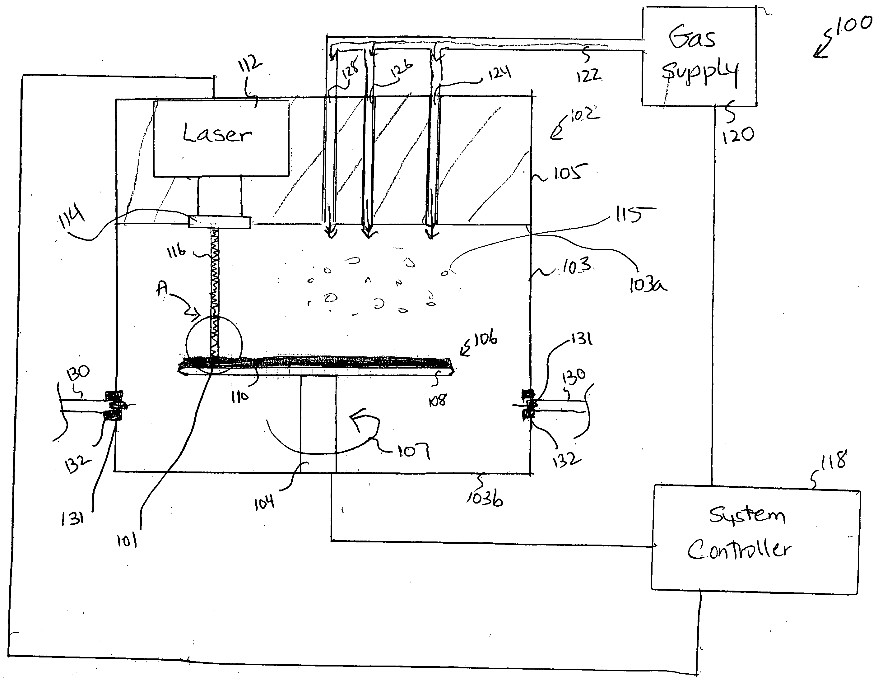
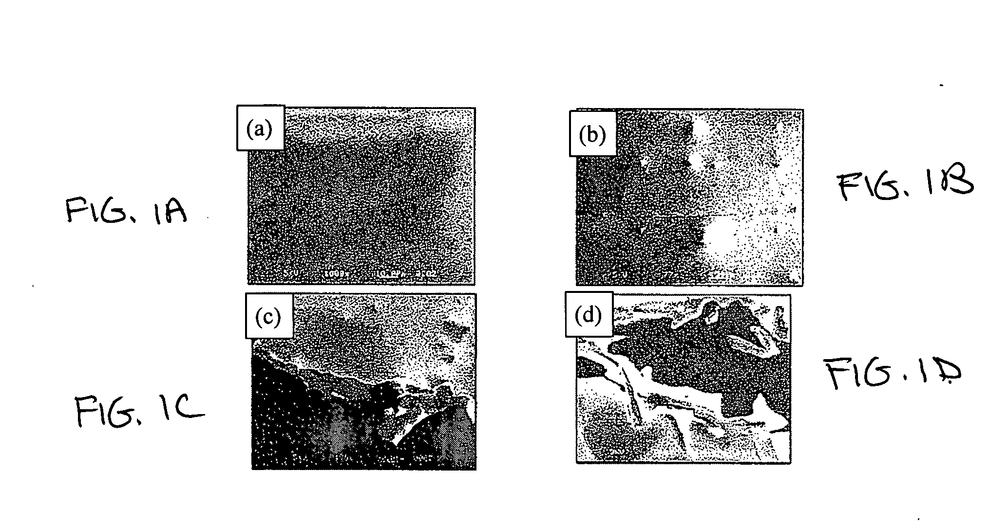
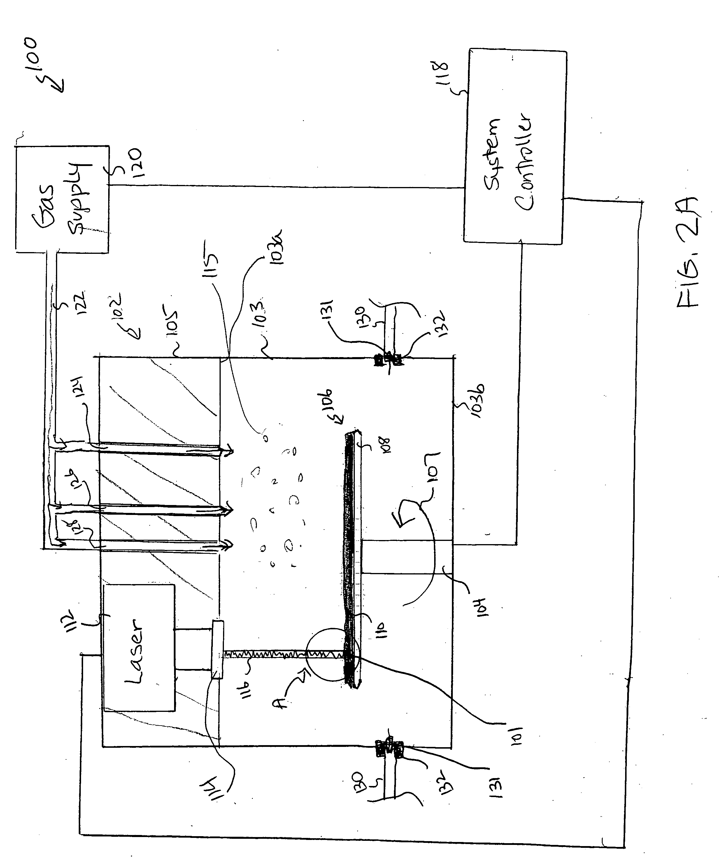
[0033] An invention that is capable of precisely and discretely removing particulate contaminants, films, and coatings from over surfaces of the substrate without substantially damaging substrate surfaces is provided. In one embodiment, high intensity ultra short laser beam pulses issued by a laser system is implemented to break a bond between the particulate contaminants / films / coatings and the substrate surface leading to the removal of the particulate contaminants, films, and coatings from over substrate surfaces. According to one example, an irradiation wavelength of the laser beam is selected such that the laser beam can be absorbed completely by the substrate while is absorbed minimally (if any) by the particulate contaminants / films / coatings being removed. In one example, the laser beam pulse duration can range between about one (1) femtosecond and 100,000 femtoseconds. In the following description, numerous specific details are set forth in order to provide a thorough understa...


PUM

PropertyMeasurementUnit
wavelengthsaaaaaaaaaa
thresholdaaaaaaaaaa
energy thresholdaaaaaaaaaa

Abstract

A substrate preparation method is provided. The method includes providing a substrate to be prepared. The substrate has a first layer and a second layer. The first layer is to be removed from over the second layer. An energy frequency that is to be absorbed by the second layer while penetrating through the first layer transparently is determined. Energy that has the determined energy frequency is applied onto the first layer so as to disrupt a bond between the first layer and the second layer at a location of application of the energy. A portion of the first layer defined at the location of application of energy is removed. A substrate preparation apparatus is also provided.

Description

BACKGROUND [0001] 1. Field of the Invention [0002] The present invention relates generally to substrate preparation and cleaning, and more particularly, to systems, apparatus, and methods for improving substrate preparation and / or cleaning operations. [0003] 2. Description of the Related Art [0004] The fabrication of semiconductor devices involves numerous processing operations. These operations include, for example, dopant implants, gate oxide generation, inter-metal oxide depositions, metallization depositions, photolithography patterning, etching operations, chemical mechanical polishing (CMP), etc. Some processing operations may include removing of an entire layer of film / coating or a discrete portion of the film / coating from over the wafer surfaces. Other processing operations may include generating particulate contaminants, which can typically adhere to wafer surfaces. Generally, particulate contaminants consist of tiny bits of distinctly defined material having an affinity to...

Claims


Application Information

Patent Timeline
Patent Type & Authority Applications(United States)
IPC IPC(8): C23F1/00H01L21/306B44C1/22C03C15/00
CPCB23K26/0069B23K26/409H01L21/0209H01L21/31116B23K26/40B23K26/356B23K2103/172
Inventor MIKHAYLICHENKO, KATRINAYAKOVLEV, VLADISLAVRAVKIN, MICHAELLARIOS, JOHN M. DEREDEKER, FRITZ C.
Owner LAM RES CORP
Why Eureka
Try Eureka