Method of manufacturing a semiconductor device

a manufacturing method and semiconductor technology, applied in the direction of manufacturing tools, solid-state devices, welding apparatus, etc., can solve the problems of difficulty in mounting, electric short circuit, and increase in manufacturing costs, and achieve the effect of minimization of semiconductor devices

Inactive Publication Date: 2006-06-22
RENESAS TECH CORP
View PDF13 Cites 6 Cited by
  • Summary
  • Abstract
  • Description
  • Claims
  • Application Information

AI Technical Summary

Benefits of technology

[0012] A purpose of the present invention is to offer a manufacturing method of a semiconductor device which can form a projection electrode easily in the case of a narrow pad pitch.
[0013] Another purpose of the present invention is to offer a manufacturing method of a semiconductor device which can realize miniaturization of the semiconductor device.

Problems solved by technology

However, when the pitch between the projection electrodes is very narrow, the present inventors found out that the following problems arose.
In this respect, if reflow treatment is performed with the mask for printing being interposed, there are problems that the mask for printing is deformed by heat and that the mask for printing under heated state possibly gives damage to the semiconductor wafer to which reflow treatment is performed next, whereby it is necessary to prepare a plurality of masks for printing.
For this reason, the manufacturing cost will increase.
If reflowing is performed under these conditions, an electric short circuit occurs among bumps and poses a problem.
In the above-mentioned ball transfer method, since there are many balls and they are small, the difficulty of mounting poses a problem.
Furthermore, in the case of the ball transfer method, since the ball diameter is for example φ 0.3 mm, which is larger than that in a screen printing method because the solder bump is formed beforehand and then is transferred to the electrode of a semiconductor wafer, it is disadvantageous for the miniaturization of a package.
That is, compared with a screen printing method, it is difficult to apply one solder bump correctly to one electrode.

Method used


Image

  • Method of manufacturing a semiconductor device
  • Method of manufacturing a semiconductor device
  • Method of manufacturing a semiconductor device

Examples


embodiment 1

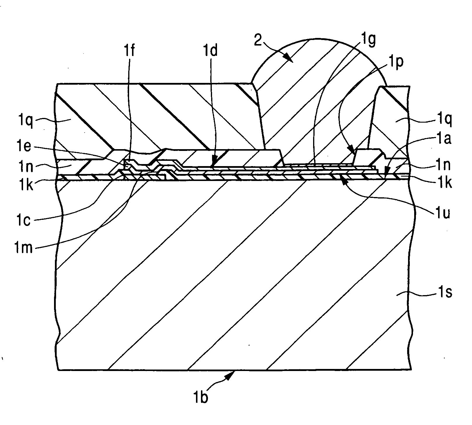
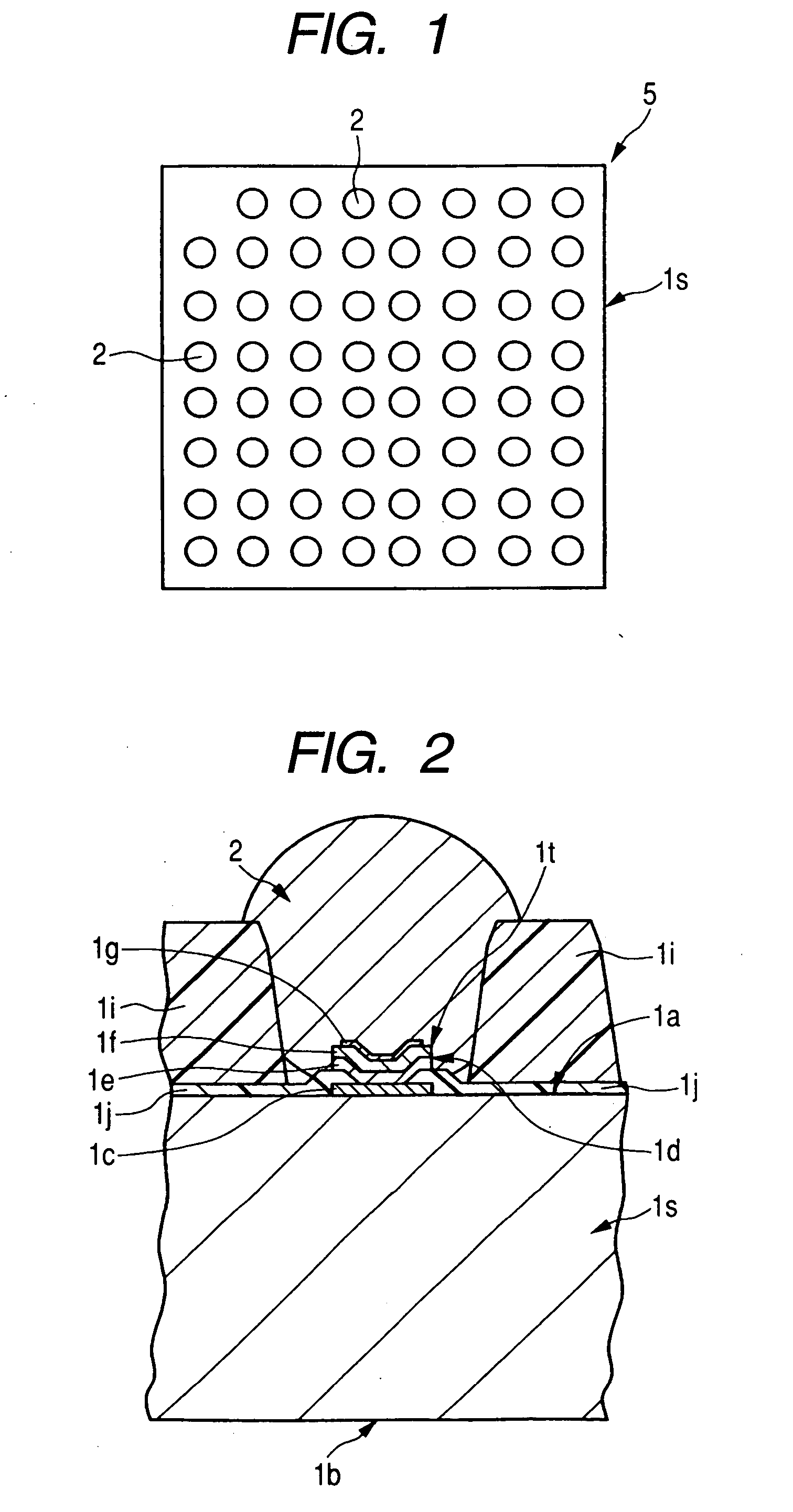
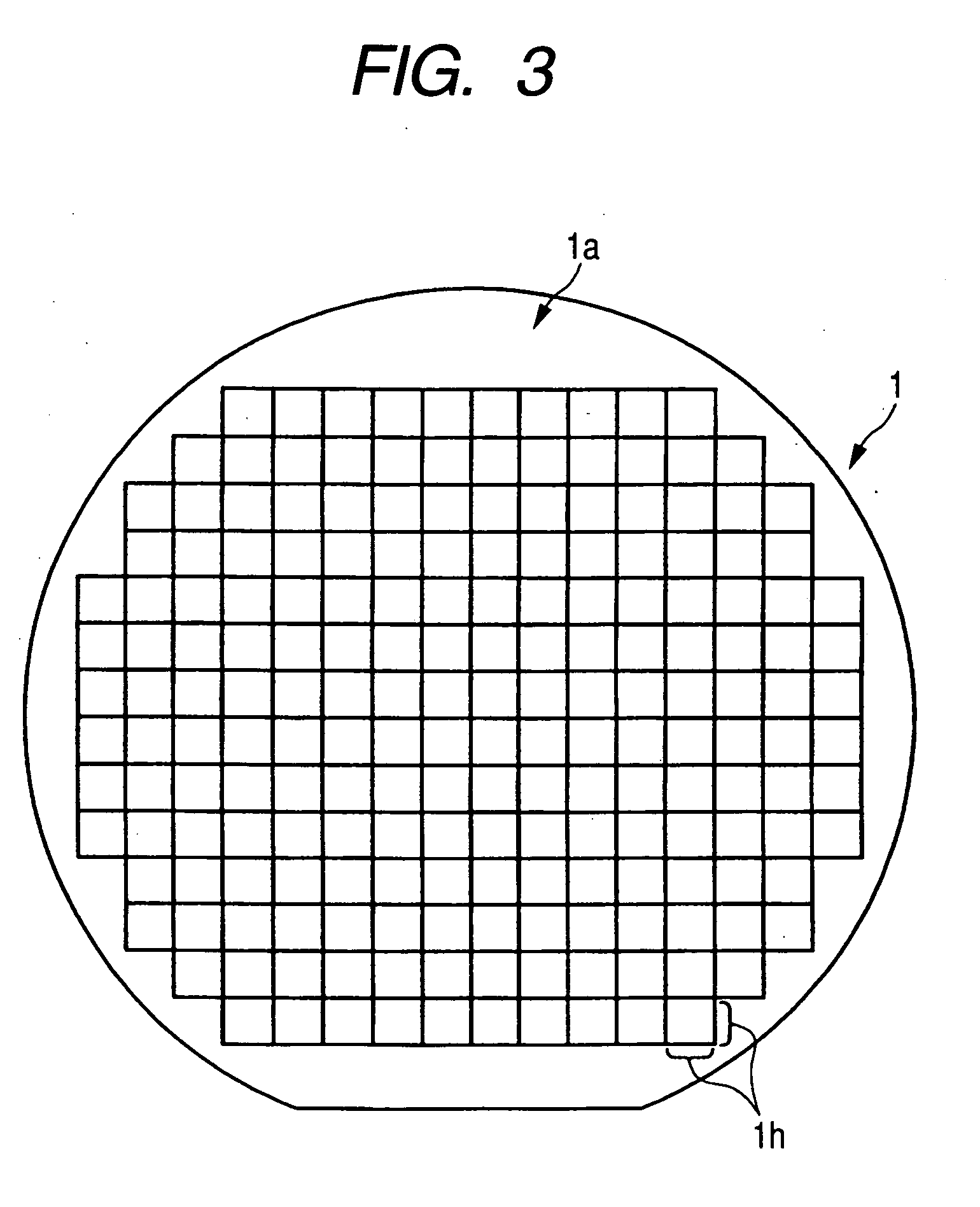
[0041]FIG. 1 is a plan view showing an example of the structure of the semiconductor device of Embodiment 1 of the present invention, FIG. 2 is an enlarged partial sectional view showing an example of the structure of the solder bump of the semiconductor device shown in FIG. 1, FIG. 3 is a plan view showing an example of the structure of the semiconductor wafer used for the assembly of the semiconductor device shown in FIG. 1, FIG. 4 is a manufacture process flow chart showing an example of the assembly procedure up to the insulating layer formation in manufacture of the semiconductor device shown in FIG. 1, FIG. 5 is a manufacture process flow chart showing an example of the assembly procedure of the soldering paste material application in manufacture of the semiconductor device shown in FIG. 1, FIG. 6 is a plan view showing an example of the structure of the semiconductor wafer after the solder bump formation in manufacture of the semiconductor device shown in FIG. 1, FIG. 7 is an...

embodiment 2

[0092]FIG. 13 is a manufacture process flow chart showing an example of the assembly procedure up to the insulating layer formation in manufacture of the semiconductor device of Embodiment 2 of the present invention, and FIG. 14 is a manufacture process flow chart showing an example of the assembly procedure of the soldering paste material application in manufacture of the semiconductor device of Embodiment 2 of the present invention.

[0093] The manufacturing method of the semiconductor device of Embodiment 2 explains the formation method of the insulating layer arranged between adjoining bump lands 1u connected to pad 1c, and the application of soldering paste material 4 on main surface 1a of semiconductor wafer 1 as an example of a bump formation method.

[0094] First, semiconductor wafer 1 as shown in the FIG. 3 which has main surface 1a, back surface 1b which is opposite to main surface 1a, and an integrated circuit formed on main surface 1a is prepared. Then, first insulating la...

embodiment 3

[0110]FIG. 15 is a manufacture process flow chart showing an example of the assembly procedure up to the insulating layer formation in manufacture of the semiconductor device of Embodiment 3 of the present invention, and FIG. 16 is a manufacture process flow chart showing an example of the assembly procedure of the soldering paste material application in manufacture of the semiconductor device of Embodiment 3 of the present invention.

[0111] The manufacturing method of the semiconductor device of Embodiment 3 explains the formation method of the insulating layer arranged between adjoining bump lands 1u connected to pad 1c, and the application of soldering paste material 4 on main surface 1a of semiconductor wafer 1 as an example of a bump formation method.

[0112] First, semiconductor wafer 1 as shown in FIG. 3 which has main surface 1a, back surface 1b opposite to main surface 1a, and an integrated circuit formed on the main surface 1a is prepared. Then, first insulating layer 1k wh...


PUM

PropertyMeasurementUnit
diameteraaaaaaaaaa
diameteraaaaaaaaaa
distanceaaaaaaaaaa

Abstract

Realization of the projection electrode formation with a narrow pad pitch is planned. In preparing a semiconductor wafer, by forming a polyimide film, which does not cover each of a plurality of lands, between the respective lands which adjoin each other among the plurality of lands on the main surface of the semiconductor wafer, applying a soldering paste material with the printing method via the mask for printing on each of a plurality of lands after polyimide film formation, and forming a solder bump by performing heat curing of the soldering paste material after removing the mask for printing, a solder bump can be formed without generating a electric short circuit between bumps even in the case of a narrow pad pitch.

Description

CROSS-REFERENCE TO RELATED APPLICATION [0001] The present application claims priority from Japanese patent application No. 2004-366029 filed on Dec. 17, 2004, the content of which is hereby incorporated by reference into this application. [0002] 1. Field of the Invention [0003] The present invention relates to manufacturing technology of a semiconductor device, and particularly relates to an effective technology in the application to the bump formation with a narrow pad pitch. [0004] 2. Description of the Background Art [0005] In the mounting method of a BGA package, as a mounting process in which the soldering joint of a solder bump formed in the BGA package and a land wired on a printed circuit board is performed, soldering paste is printed on the land wired on the printed circuit board through the opening of a hole made in a mask plate, by putting the mask on the printed circuit board, and applying the soldering paste on this mask. After the location of this land where the solder...

Claims


Application Information

Patent Timeline
Patent Type & Authority Applications(United States)
IPC IPC(8): B23K31/02B23K31/00
CPCB23K3/0623H01L24/02H01L24/03H01L24/05H01L24/11H01L24/12H01L2224/0401H01L2224/05083H01L2224/05624H01L2224/1147H01L2224/11472H01L2224/1148H01L2224/13006H01L2224/13022H01L2224/13099H01L2924/01004H01L2924/01013H01L2924/01015H01L2924/01029H01L2924/01075H01L2924/01078H01L2924/01079H01L2924/014H01L2924/14H01L2924/00014H01L2924/01005H01L2924/01006H01L2924/01033
Inventor SHIGIHARA, HIROMISHIGIHARA, HISAOYAJIMA, AKIRA
Owner RENESAS TECH CORP
Why Eureka
Try Eureka