Packaged chip capable of lowering characteristic impedance

Inactive Publication Date: 2006-06-22
DOMINTECH
View PDF8 Cites 19 Cited by
  • Summary
  • Abstract
  • Description
  • Claims
  • Application Information

AI Technical Summary

Benefits of technology

[0004] This invention is mainly to provide a packaged chip capable of lowering characteristic impedance and particularly lowers electrical noises and EMI with a designed metal layer of structure at a specified area of a lead-wire frame, namely with an improved lead wire connection structure and may eliminate a problem of poor transmission of signals resulting from characteristic impedance of a packaged body so that the stable transmission of signals and the efficient transmission speed may be further developed.
[0005] From the object mentioned above, according to an embodiment of this invention, a chip, a lead wire frame, a plurality of metal layers, adhesive layers, lead wires, and a mold are structured and molded into TSOP LOC and thin-small-sized packaging (including TSOP and QFP) types; thereby

Problems solved by technology

From the mentioned-above disclosed chip TSOP or QFP and TSOP LOC types, solutions to Electromagnetic Interference (EMI) and noises, including a shot noise, a flicker noise, a surge noise, a thermal noise, an allocation noise and the like, often caused in electronic products are

Method used


Image

  • Packaged chip capable of lowering characteristic impedance
  • Packaged chip capable of lowering characteristic impedance
  • Packaged chip capable of lowering characteristic impedance

Examples


Embodiment Construction

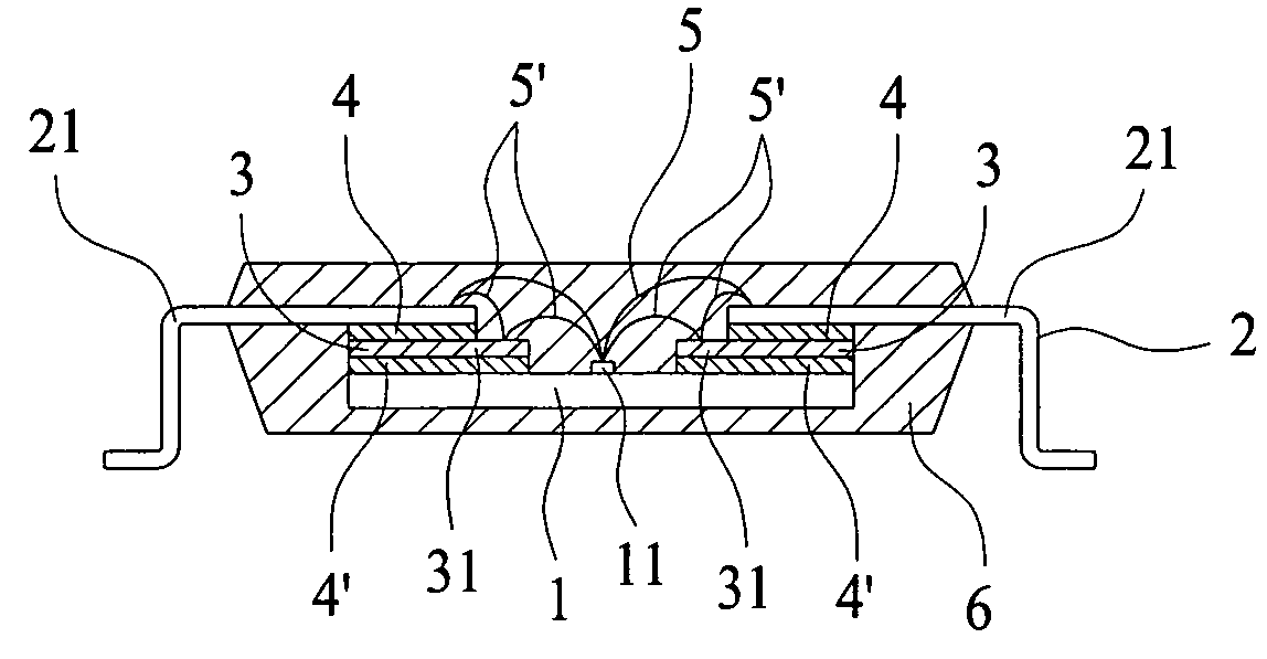
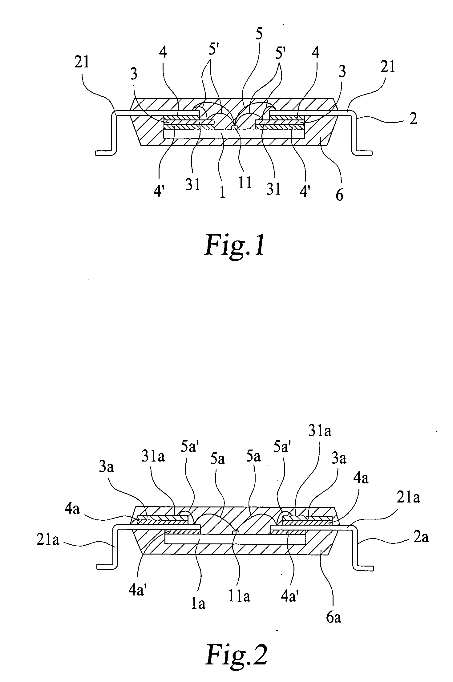
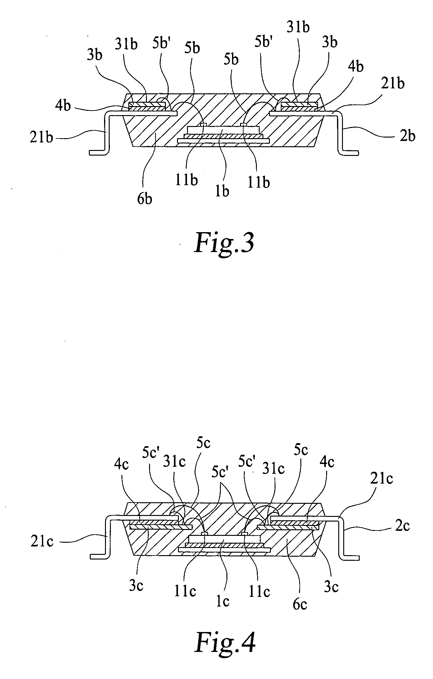
[0014] Referring now to FIGS. 1 and 5, this invention is a packaged chip capable of lowering characteristic impedance, comprising a chip 1, a lead wire frame 2, a plurality of metal layers 3, adhesive layers 4 and 4′, lead wires 5 and 5′, and a mold 6, in which the chip 1 is a specifically functional electronic element made of silicon or GaAs semiconductor material and a plurality of electrode contacts 11 are provided at a specified site; the lead wire frame 2 is structured with metallic materials stamped into 2 or 4 rows (QFP type) of a plurality of leads 21 to serve as the outward electrically connecting elements of the chip 1; the metal layers 3 are metallic tablets, films, or nets, or other conductive tablets; the adhesive layers 4 and 4′ may be formed into adhesive solid substances (glue and the like) or adhesive tapes after they are dried from the liquid state; the lead wires 5 and 5′ are metallic or conductive wires; and the mold 6 is an insulator wrapping the formerly descri...


PUM


Abstract

A packaged chip lowering characteristic impedance comprises a chip, a lead wire frame, a plurality of metal layers, adhesive layers, lead wires, and a mold, being formed into TSOP LOC and thin-small-sized packaging types; from a specified site above or under each row of leads of the lead wire frame, metal layers are fixed respectively with adhesives layers to the lead wire frame; lead wires are connected respectively between electrode contacts of the chip and leads of the lead wire frame and a lead wire provided is connected between at least one lead and the metal layer, so the packaged chip using metal layers as a Ground or Power plane is formed; thus, electrical noises and EMI are lowered and a problem of poor transmission of signals is eliminated so that a stable transmission of signals and an efficient transmission speed may be further developed.

Description

FIELD OF THE INVENTION [0001] This invention relates to a packaged chip capable of lowering characteristic impedance and particularly to an improvement of structures of a thin-small-outline-package lead-on-chip (TSOP LOC) type and thin-small-outline-package and quad flat pack (TSOP and QFP) types. BACKGROUND OF THE INVENTION [0002] A conventional chip packaging types are generally a thin-small-outline-package or a quad flat pack type (TSOP or QFP as shown in FIG. 8) and a thin-small-outline-package lead-on-chip (TSOP LOC as shown in FIG. 7) in structure and both of the two structures have chips 10 and 10′ on which lead wire frames 20 and 20′ outward conductive are provided; the lead wire frame 20 is a metallic material stamped into 2 or 4 rows of a plurality of arranged leads 201 and 201′, and thereby bonding wires 40 and 40′ electrically connected to each other are provided between the plurality of leads 201 and 201′ of electrode contacts and lead wire frames 20 and 20′ of the chip...

Claims


Application Information

Patent Timeline
IPC IPC(8): H01L23/34H01L23/28H01L23/495
CPCH01L23/4951H01L23/49527H01L24/49H01L2224/48091H01L2224/48247H01L2224/4826H01L2224/49109H01L2224/4911H01L2224/49171H01L2224/73215H01L2224/73265H01L2924/01014H01L2924/01057H01L2924/01082H01L2924/10329H01L2924/3011H01L2924/00014H01L2924/00H01L2224/32245H01L24/48H01L2924/181H01L2224/45099H01L2224/05599H01L2924/00012
Inventor TZU, CHUNG-HSING
Owner DOMINTECH
Why Eureka
Try Eureka