Method for forming quantum dots

a quantum dot and etching technology, applied in the field of forming quantum dots, can solve the problems of inability to precisely control the size low optical quality of the quantum dot, and inferring complicated physical and optical properties

Inactive Publication Date: 2006-06-22
HON HAI PRECISION IND CO LTD
View PDF4 Cites 19 Cited by
  • Summary
  • Abstract
  • Description
  • Claims
  • Application Information

AI Technical Summary

Benefits of technology

[0011] Compared with the conventional methods, the present method does not use a photolithography technique thus reduces or even avoids the possibility of forming various surface states. Furthermore, a potential effect of the thermal expansion coefficient of the metal is finite over the temperature range involved and thus the size of the nanopores, which are restricted by the metal layer, is essentially cons

Problems solved by technology

The surface states are sources of non-radiative recombination centers, and presence of such centers would lower the optical quality of the quantum dots.

Method used


Image

  • Method for forming quantum dots
  • Method for forming quantum dots

Examples


Embodiment Construction

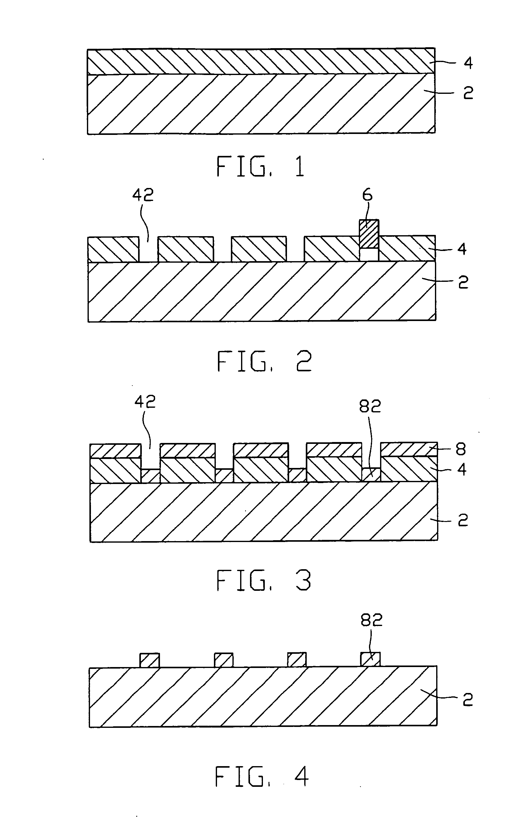
[0019] Reference will now be made to the drawings to describe embodiments of the present method, in detail.

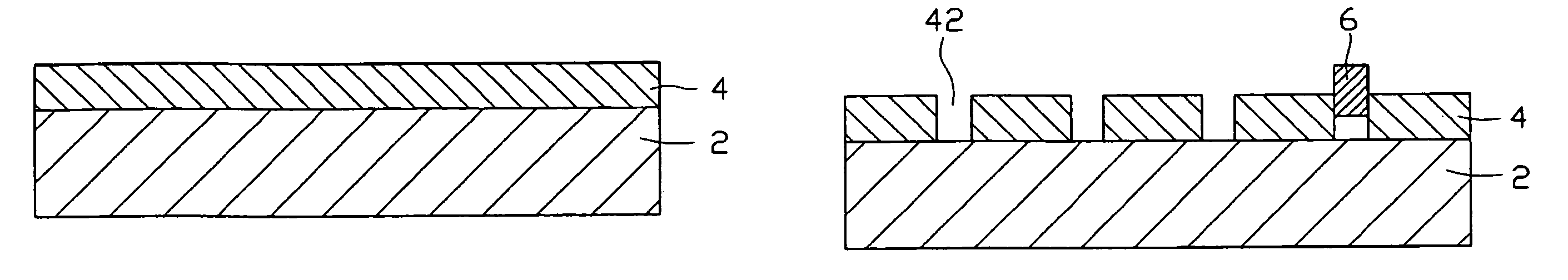
[0020] Referring to FIGS. 1, 2, 3 and 4, a method for forming quantum dots includes the following steps: (a) depositing a metal layer 4 on a substrate 2; (b) using an atomic force microscope (AFM) probe 6 to form a plurality of nanopores 42 in the metal layer 4; (c) depositing a semiconductor layer 8 on the metal layer 4 and in the nanopores 42; and (d) removing the metal layer 4 and the portions of the semiconductor layer 8 located on the metal layer 4, thereby forming a plurality of quantum dots 82 on the substrate 2.

[0021] Referring to FIG. 1, in step (a), the substrate 2 is made of semiconductor material, such as silicon, germanium, gallium arsenide, indium gallium nitride, gallium nitride, indium nitride, and so on. In the preferred embodiment, the substrate 2 is made of silicon. The metal layer 4 has finite thermal expansion coefficient and can, advantageously, be a gol...


PUM


Abstract

A method for forming quantum dots includes the following steps: (a) depositing a metal layer (4) on a substrate (2); (b) using an atomic force microscope (AFM) probe (6) to form a plurality of nanopores (42) in the metal layer (4); (c) depositing a semiconductor layer (3) on the metal layer and in the nanopores; and (d) removing the metal layer and the portions of the semiconductor layer located on the metal layer, thereby forming a plurality of quantum dots (82) on the substrate. The method does not use a photolithography technique, thus reduces or even avoids the possibility of forming various surface states. Furthermore, a potential effect of the thermal expansion coefficient of the metal is finite over the temperature range involved and thus the size of the nanopores, which are restricted by the metal layer, is essentially constant. Therefore, a size of the quantum dots is controllable.

Description

BACKGROUND [0001] 1. Field of the Invention [0002] This invention relates generally to methods for manufacturing semiconductor devices and, more specifically, to a method for forming quantum dots. [0003] 2. Discussion of Related Art [0004] Quantum dots are effectively zero-dimensional quantum structures. A quantum dot has a typical size of about 10 nanometers. The extreme sizes of quantum dots results in unique physical and optical properties from that of macro-materials. For example, the color of quantum dot can be easily tuned to different wavelength by simply changing the size of the dots. The principle behind this unique property is the quantum confinement effect. Thus, quantum dots are one of the most promising candidates for future high performance devices in communication systems, biomedical fields, sensors, detectors, and optical systems. [0005] Conventional techniques for forming quantum dots are based on quantum well structures. One of those methods includes the following ...

Claims


Application Information

Patent Timeline
IPC IPC(8): H01L21/00
CPCB82Y10/00G01Q80/00H01L29/127H01L29/0673H01L29/0676H01L29/0665
Inventor LIN, MONG-TUNG
Owner HON HAI PRECISION IND CO LTD
Why Eureka
Try Eureka