Multilayer printed wiring board

a printing board and multi-layer technology, applied in the direction of printed circuit stress/warp reduction, dielectric characteristics, cross-talk/noise/interference reduction, etc., can solve the problems of difficult calcination and make a high dielectric constant material into a ceramic, and achieve the effect of reducing the degradation of the decoupling effect, prolonging the wiring, and reducing the difficulty of calcination

Active Publication Date: 2006-06-29
IBIDEN CO LTD
View PDF13 Cites 65 Cited by
  • Summary
  • Abstract
  • Description
  • Claims
  • Application Information

AI Technical Summary

Benefits of technology

[0007] In this multilayer printed wiring board, the high dielectric constant layer of the layered capacitor portion, which is connected between the power supply line and the ground line, is formed of ceramic. In this structure, the dielectric constant and the static capacitance can be high, compared with those in the conventional arrangement that uses an organic resin blended with inorganic filler. Therefore, an adequate decoupling effect is exhibited even when the on / off frequency of the semiconductor element is high and in the range of several GHz to several dozen GHz (for example, 3 GHz to 20 GHz).
[0019] The multilayer printed wiring board of the invention may have a stress relaxing portion formed of an elastic material and disposed between the mounting portion and the layered capacitor portion. In this structure, even if stress occurs due to a thermal expansion difference between the semiconductor element mounted on the mounting portion and the layered capacitor portion or the build-up portion, the stress relaxing portion absorbs the stress. Thus, the reliability of connection, the reliability of insulation, etc. will thus not readily lowered. Also, though the high dielectric constant layer of the layered capacitor portion is thin, brittle, and thus tends to crack readily, the forming of cracks can be prevented by the presence of the stress relaxing portion. Here, the stress relaxing portion may be formed just below the semiconductor element that is mounted on the above-described mounting portion. Since stress due to a thermal expansion difference mainly becomes a problem below the semiconductor element, the material cost can be held down by forming the stress relaxing portion below the semiconductor element. The material of such a stress relaxing portion is not restricted in particular, but may be a modified epoxy based resin sheet, a polyphenylene ether based resin sheet, a polyimide based resin sheet, a cyanoester based resin sheet, an imide based resin sheet, and other organic base resin sheets. Such an organic based resin sheet may contain a thermoplastic resin, such as a polyolefin based resin or a polyimide based resin, a thermosetting resin, such as silicone resin, or a rubber based resin, such as SBR, NBR, urethane, etc., and may contain a fibrous, filler, or flattened inorganic based material of silica, alumina, zirconia, etc. The stress relaxing portion preferably has a Young's modulus in a range of 10 to 1000 MPa. When stress occurs due to a thermal expansion coefficient difference between the semiconductor element mounted on the mounting portion and the layered capacitor portion, the stress relaxing portion within this range can adequately relax the stress.

Problems solved by technology

A build-up portion is generally prepared under a temperature condition of not more than 200° C., and it is difficult to calcine and make a high dielectric constant material into a ceramic.

Method used


Image

  • Multilayer printed wiring board
  • Multilayer printed wiring board
  • Multilayer printed wiring board

Examples


example 2

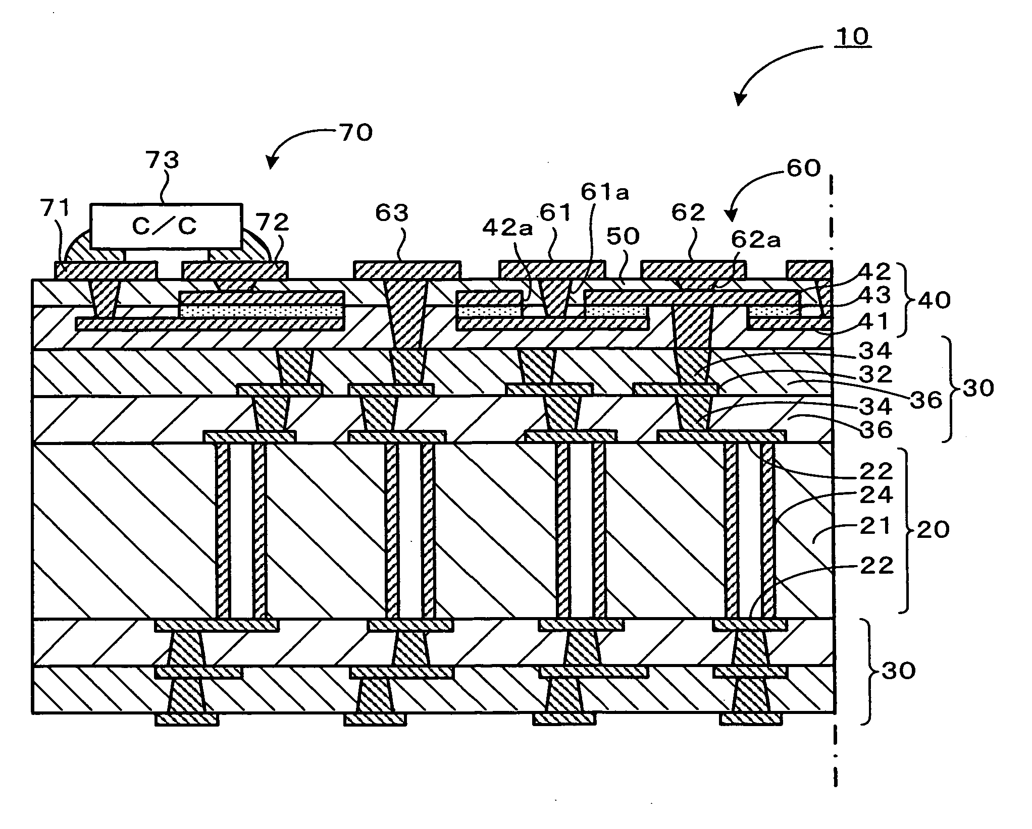
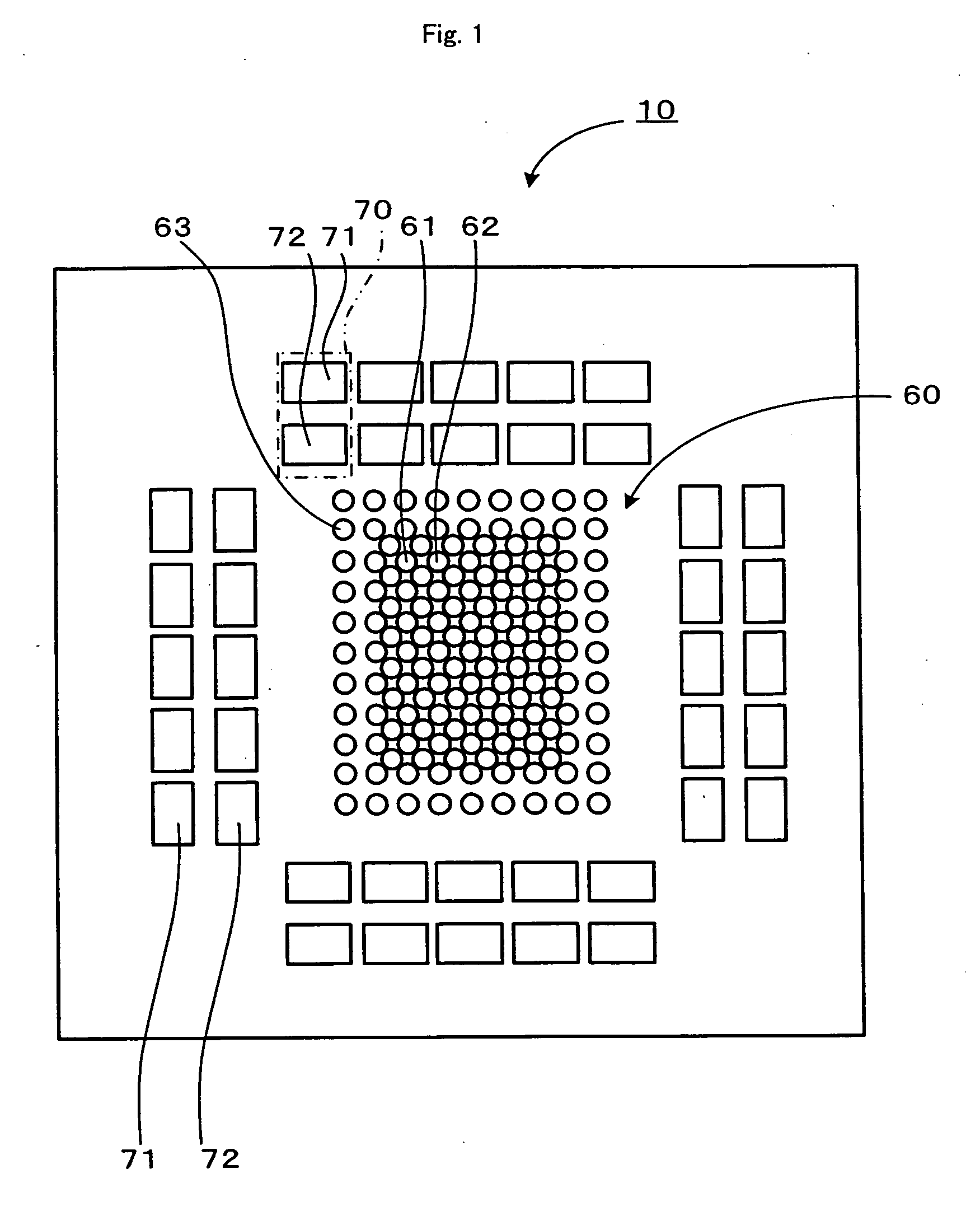
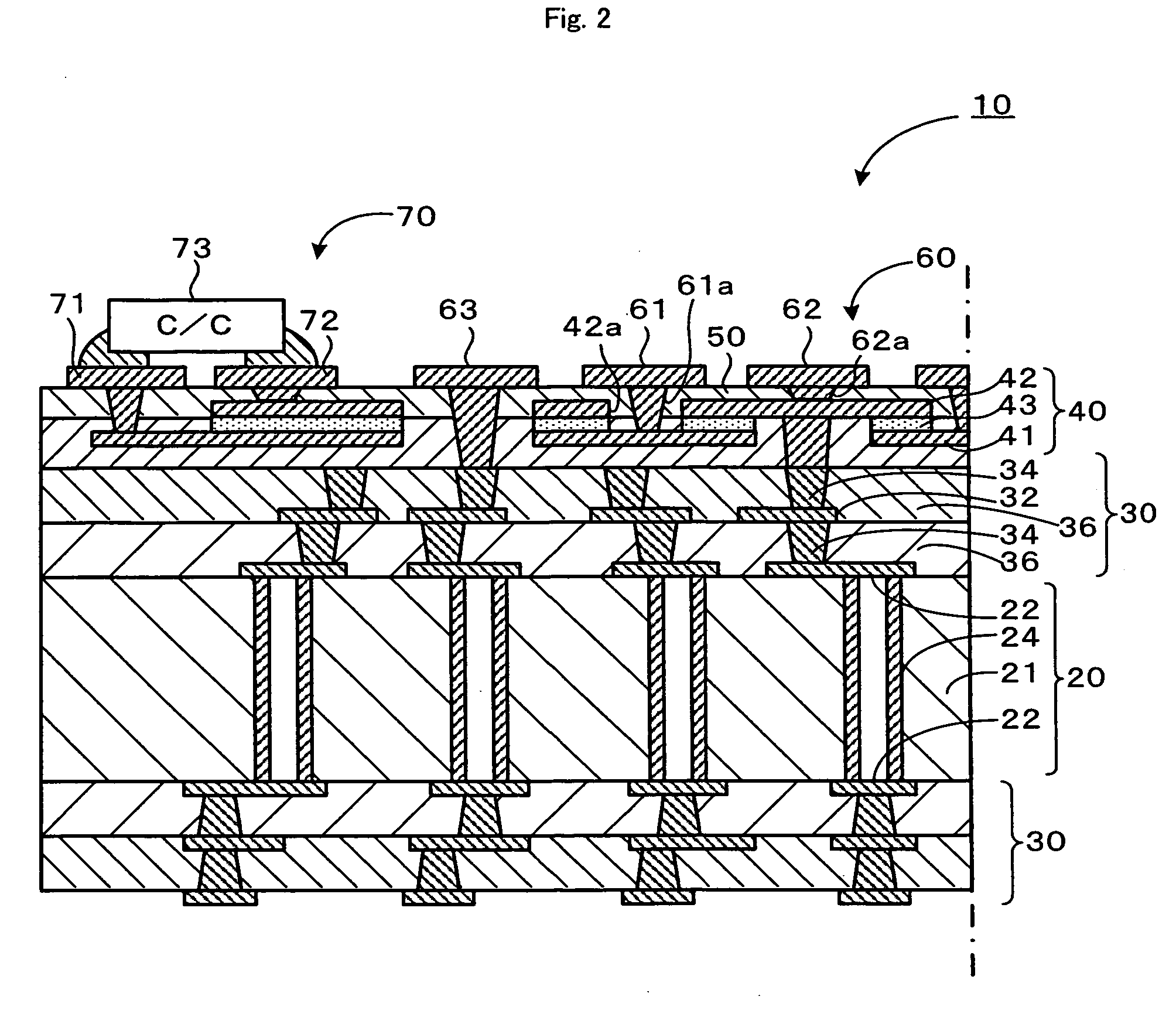
[0063]FIG. 8 is a longitudinal section (showing only the left side of a central line) of a multilayer printed wiring board 110 of Example 2. As shown in FIG. 8, the multilayer printed wiring board 110 of the present example has the same core substrate 20 as Example 1, the build-up portion 30 in which wiring patterns 32 and 22 laminated via resin insulating layer 36 on the upper surface of core substrate 20 are electrically connected by via holes 34, an interlayer insulating layer 120, laminated on the build-up portion 30, a layered capacitor portion 140, laminated on the interlayer insulating layer 120 and arranged with a high dielectric constant layer 143 and the first and second layer electrodes 141 and 142 that sandwich the high dielectric constant layer 143, a stress relaxing portion 150, laminated on the high dielectric constant layer 143 and formed of an elastic material, a mounting portion 160, on which a semiconductor element is mounted, and the chip capacitor positioning re...

example 3

[0089]FIG. 13 is a longitudinal section (showing only the left side of a central line) of a multilayer printed wiring board 210 of an Example 3. As shown in FIG. 13, the multilayer printed wiring board 210 of the present example has the same core substrate 20 as Example 1, the build-up portion 30 in which wiring patterns 22 and 32 laminated via the resin insulating layer 36 at the upper surface of the core substrate 20 are electrically connected by means of via holes 34, an interlayer insulating layer 220, laminated on the build-up portion 30, a layered capacitor portion 240, laminated on interlayer insulating layer 220 and arranged with a high dielectric constant layer 243 and the first and second layer electrodes 241 and 242 that sandwich the high dielectric constant layer 243, an interlayer insulating layer 245, laminated on the layered capacitor portion 240, a stress relaxing portion 250, formed of an elastic material and laminated on the interlayer insulating 245, a mounting po...

example 4

[0105] In Example 2, all of through holes 530 and through holes 531 were formed at positions corresponding to the power supply pads and the ground pads. As a result, the static capacitance of the layered capacitor portion became 0.4 pF.


PUM


Abstract

A multilayer printed wiring board 10 includes: a mounting portion 60 on the top surface of which is mounted a semiconductor element that is electrically connected to a wiring pattern 32, etc.; and a capacitor portion 40 having a high dielectric constant layer 43, formed of ceramic and first and second layer electrodes 41 and 42 that sandwich the high dielectric constant layer 43. One of either of the first and second layer electrodes 41 and 42 is connected to a power supply line of the semiconductor element and the other of either of the first and second layer electrodes 41 and 42 is connected to a ground line. In this multilayer printed wiring board 10, high dielectric constant layer 43 included in the layered capacitor portion 40, which is connected between the power supply line and the ground line, is formed of ceramic. With this structure, the static capacitance of the layered capacitor portion 40 can be high, and an adequate decoupling effect is exhibited even under circumstances in which instantaneous potential drops occur readily.

Description

CROSS-REFERENCE TO RELATED APPLICATIONS [0001] This application is a continuation application of International Application No. PCT / JP2004 / 018526, filed on Dec. 6, 2004.BACKGROUND ART [0002] 1. Field of the Invention [0003] This invention concerns a multilayer printed wiring board having build-up portions, in which wiring patterns, laminated in plural layers via insulating layers, are electrically connected to each other by means of via holes in the insulating layers. [0004] 2. Description of the Prior Art [0005] Various structures have been proposed for multilayer printed wiring boards having build-up portions. In the build-up portions of the proposed multilayer printed boards, wiring patterns, laminated in plural layers via insulating layers, are electrically connected to each other by means of via holes in the insulating layers. In this type of multilayer printed wiring board, the potential of the power supply line may drop instantaneously due to switching noise when a mounted sem...

Claims


Application Information

Patent Timeline
Patent Type & Authority Applications(United States)
IPC IPC(8): H05K1/03H05K1/11H05K1/16H05K3/46
CPCH05K1/0231H05K2201/10734H05K1/113H05K1/162H05K3/4602H05K2201/0133H05K2201/0175H05K2201/0179H05K2201/0187H05K2201/09509H05K2201/09518H05K2201/09563H05K2201/096H05K2201/09718H05K2201/09763H05K2201/10522H05K1/0271H05K3/46
Inventor KARIYA, TAKASHIMOCHIDA, AKIRA
Owner IBIDEN CO LTD
Why Eureka
Try Eureka