Optical information processing apparatus

a technology of optical information processing and optical information, which is applied in the field of optical information processing apparatus, can solve the problems of difficult to accurately detect ram signals, difficult to read out ram signals, and difficulty in accurate detection of ram signals, so as to achieve accurate reading of ram signals, without reducing phase pit depth

Inactive Publication Date: 2006-06-29
FUJITSU LTD
View PDF6 Cites 1 Cited by
  • Summary
  • Abstract
  • Description
  • Claims
  • Application Information

AI Technical Summary

Benefits of technology

[0020] It is therefore the object of the present invention to provide an optical information processing apparat

Problems solved by technology

However, when the RAM signal is detected, it is disadvantageous that crosstalk is generated by an intensity modulation signal from the phase pit and that the RAM signal is buried in the ROM signals to become difficult to be read out.
However, both technologies have dependency to frequency and, as the transfer rate becomes higher,

Method used


Image

  • Optical information processing apparatus
  • Optical information processing apparatus
  • Optical information processing apparatus

Examples


first embodiment

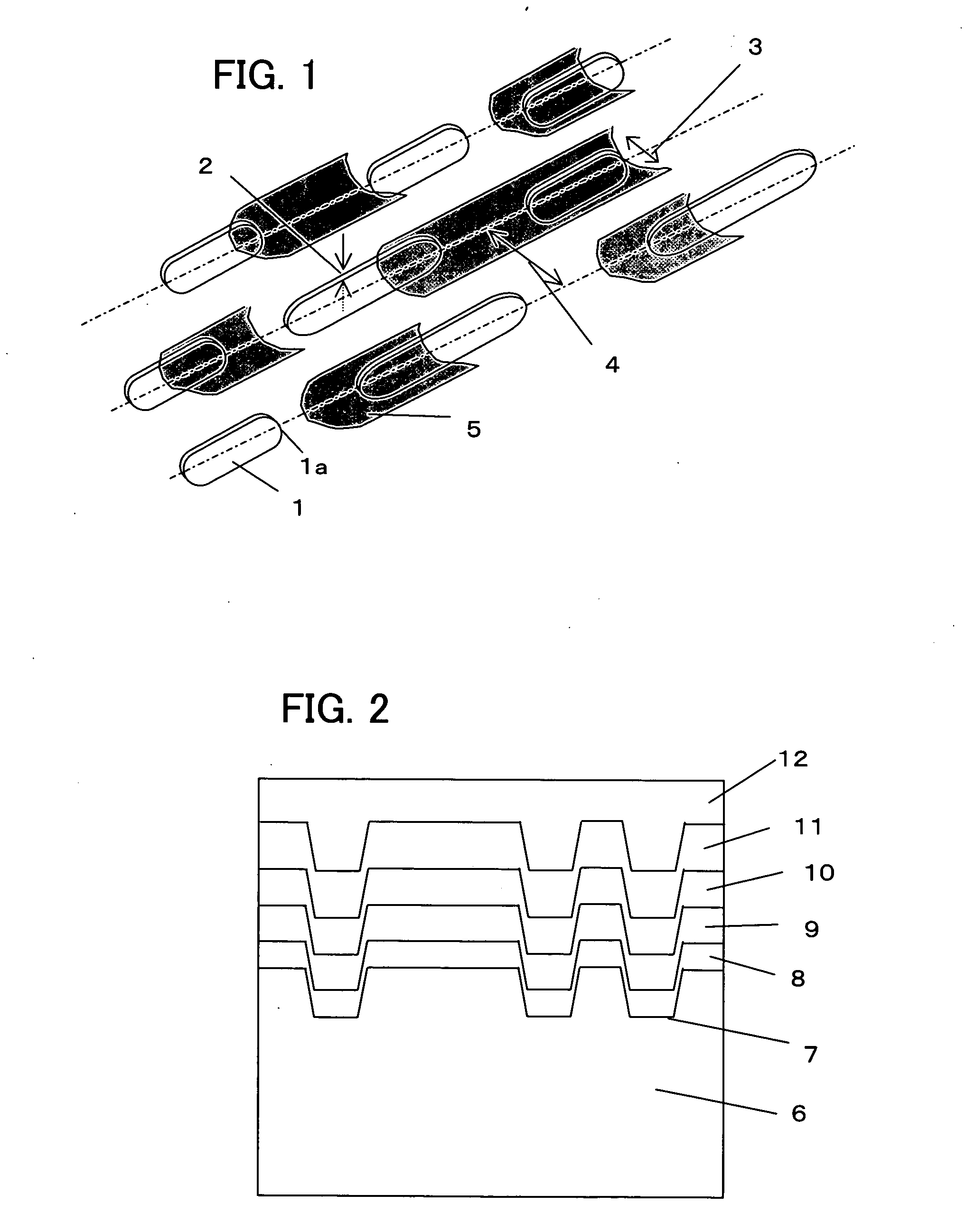
[0117] When RAM information was recorded with the EFM modulation mode and the mark length same as the ROM signal according to the present invention described above to perform jitter measurement, a RAM jitter value of about 7% was obtained in terms of clock versus data.

[0118] A ROM jitter detected from the ROM 2 signal is about 4% and a problem-free characteristic is obtained for practical use.

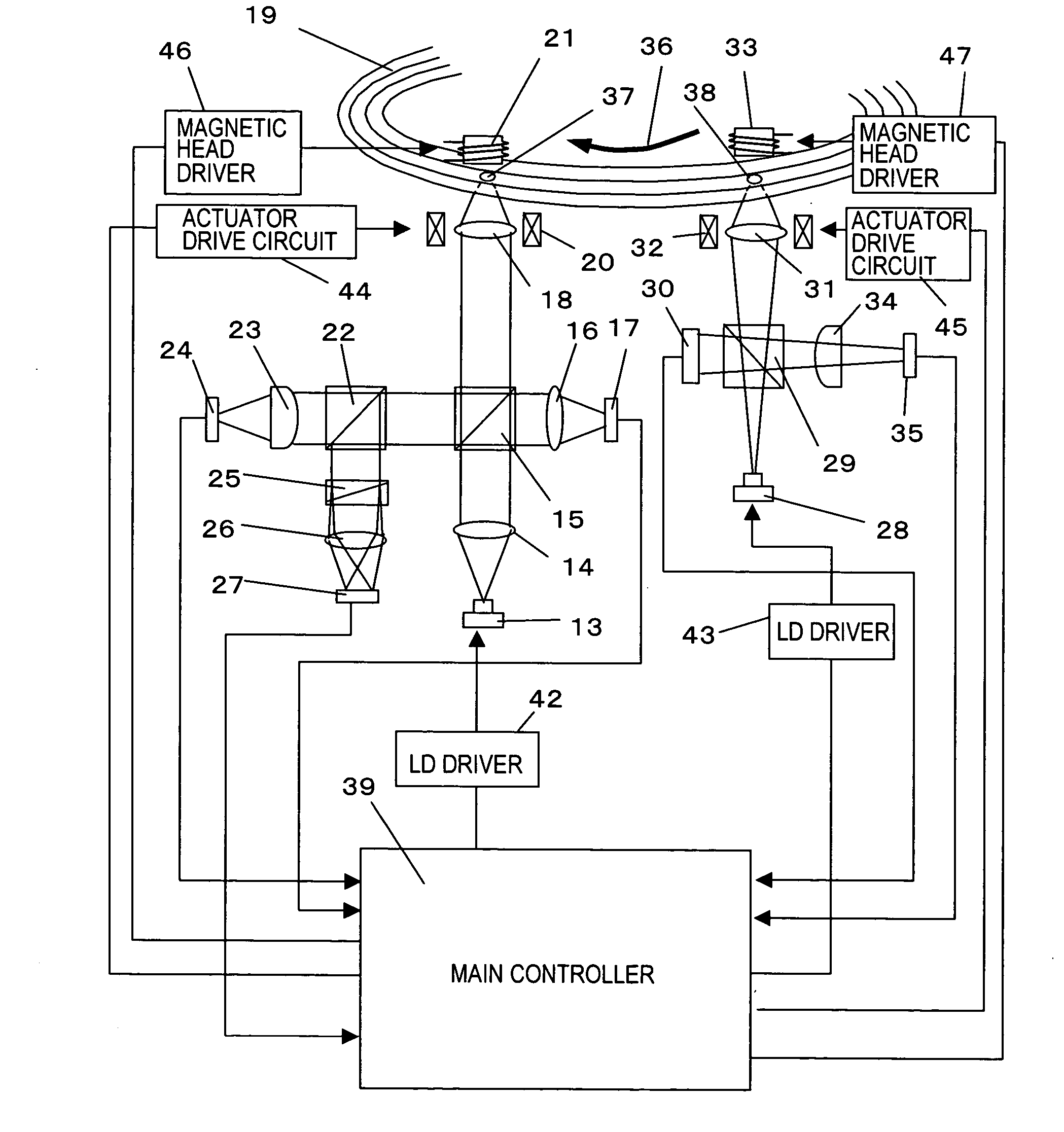
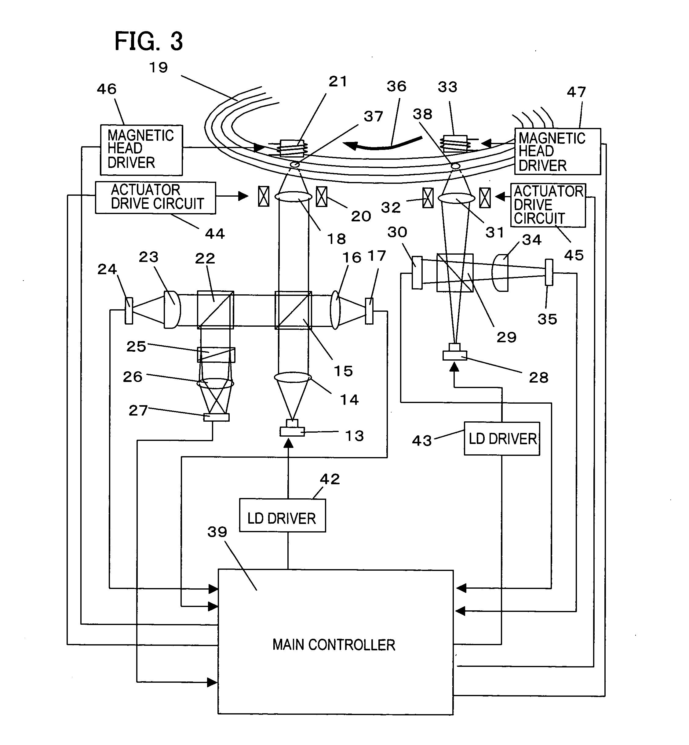
[0119]FIG. 10 is a diagram for describing an embodiment realizing a specific arrangement method for concentrating the beam spots 37 and 38 onto the same track in the information processing apparatus of FIG. 3.

[0120] Each optical system having the condenser lenses 18, 31 of FIG. 3 is disposed on a head base A5. The head base A5 can be moved by a guide rail A8 and a ball screw A7 in the direction of the radius of the optical disk which is rotated around an axis A9 by a spindle motor drive circuit A4. Specifically, the movement to the desired radial position can be performed by driving a motor A...

second embodiment

[0147] When the RAM information is detected, although in the information processing apparatus 1 shown in FIG. 3, adjustment must be needed at a portion with a long delay amount of 5.2 msec on the nsec level which is the order of the pit signal, in the information processing apparatus of the second embodiment shown in FIG. 11, since the interval between the beam spots 37 and 38 is 16 μm and a short delay amount of about 3 μsec is generated when rotating the optical disk 19 at a linear velocity of 4.8 m / sec, the delay circuit can be easily designed.

[0148] Since the integral heads 54 and 57 and the MEMS mirror 55 is used and only one (1) object lens 1 is used, the size and weight of the optical head can be dramatically reduced.

[0149] For recording of the RAM information, a floating-type magnetic head 79 with a slider is disposed at a position opposite to the object lens 74 with the optical disk 19 existing therebetween. The position of the magnetic head 38 is set to a position where a...


PUM


Abstract

For a concurrent ROM-RAM recording medium, the present invention provides an optical information processing apparatus which can accurately read a RAM signal at the time of high-speed transfer without reducing a phase pit depth. The optical information processing apparatus is an optical information processing apparatus for controlling writing and reading of information on a concurrent ROM-RAM recording medium recording ROM signal information as a phase pit on a track and magneto-optically recording RAM signal information on the phase pit, comprising an optical system for forming two (2) first and second beam spots with an interval on the same track of the recording medium; a circuit unit for modulating the first beam spot intensity with a second ROM signal read by the second beam spot; and a circuit for detecting a RAM signal from a first ROM signal read by the first beam spot.

Description

CROSS-REFERENCE TO RELATED APPLICATIONS [0001] This application is a continuation of international application PCT / JP2003 / 011822, filed on Sep. 17, 2003.TECHNICAL FIELD [0002] The present invention relates generally to an optical information processing apparatus, and more particularly, to an optical information processing apparatus using an optical element for recording and regeneration processing of ROM (fixed record) information and RAM (writable / readable record) information which are recorded and regenerated on the same recording medium. BACKGROUND ART [0003] As a technology for recording and regenerating ROM information and RAM information on the same recording medium, a concurrent ROM-RAM optical disk is known (e.g., non-patent document 1). In the concurrent ROM-RAM optical disk, a magnetic optical recording film is formed for recording and regenerating a RAM signal on a transparent substrate where a phase pit signal are formed as a ROM signal by physical concavity and convexit...

Claims


Application Information

Patent Timeline
IPC IPC(8): G11B11/00G11B7/005G11B7/007G11B7/12G11B7/123G11B7/13G11B7/131G11B7/135G11B7/1353G11B11/105
CPCG11B7/0053G11B7/0079G11B7/123G11B7/131G11B7/1353G11B11/10508G11B11/10517G11B11/10543G11B11/10554G11B11/10597
Inventor AOYAMA, NOBUHIDE
Owner FUJITSU LTD
Why Eureka
Try Eureka