
Optical device and fabrication method and apparatus for the same

a technology of optical devices and fabrication methods, applied in the field of optical devices, can solve the problems of large number of devices to be used, long assembly time, and complicated fabrication processes, and achieve the effects of reducing fabrication costs, reducing the loss of light at the joint surface, and simple fabrication process

Inactive Publication Date: 2006-06-29
PRECISE GAUCO
View PDF7 Cites 14 Cited by
  • Summary
  • Abstract
  • Description
  • Claims
  • Application Information

AI Technical Summary

Benefits of technology

[0017] The present invention has been achieved in view of the above-described problems. An object of the present invention is to provide an optical device fabrication method and an optical device fabrication apparatus capable of fabricating optical devices with high precision and reliability in a simple process and at a low cost, and an optical device fabricated by using such a fabrication method.
[0021] According to the present invention, the first optical device and the second optical device are spliced by fused-splicing, and therefore, a capillary for supporting an optical fiber and processes such as polishing of the splicing surfaces of the two optical devices and AR coating are no longer necessary. Consequently, a fabrication process is made simple and the fabrication cost can be reduced. Further, no adhesive is arranged on the joint surfaces of the first optical device and the second optical device, and therefore, it is possible to firmly splice the two optical devices without causing optical distortion such as distortion of a plane of polarization to occur. In particular, almost no air-containing layer exists between the joint surfaces of the two optical devices and the effect that stain and dust attached to the joint surfaces are removed can be expected by thermal plasma caused to occur when the splicing surface is softened, and therefore, a propagation loss of light at the joint surface and the like can be reduced. Furthermore, misalignment of the optical axis on the spliced surface caused due to the use of adhesive and temporal deterioration of the resin material of adhesive do not occur, and therefore, the reliability of the product can be improved and it is made possible to propagate light having high power through an optical fiber.
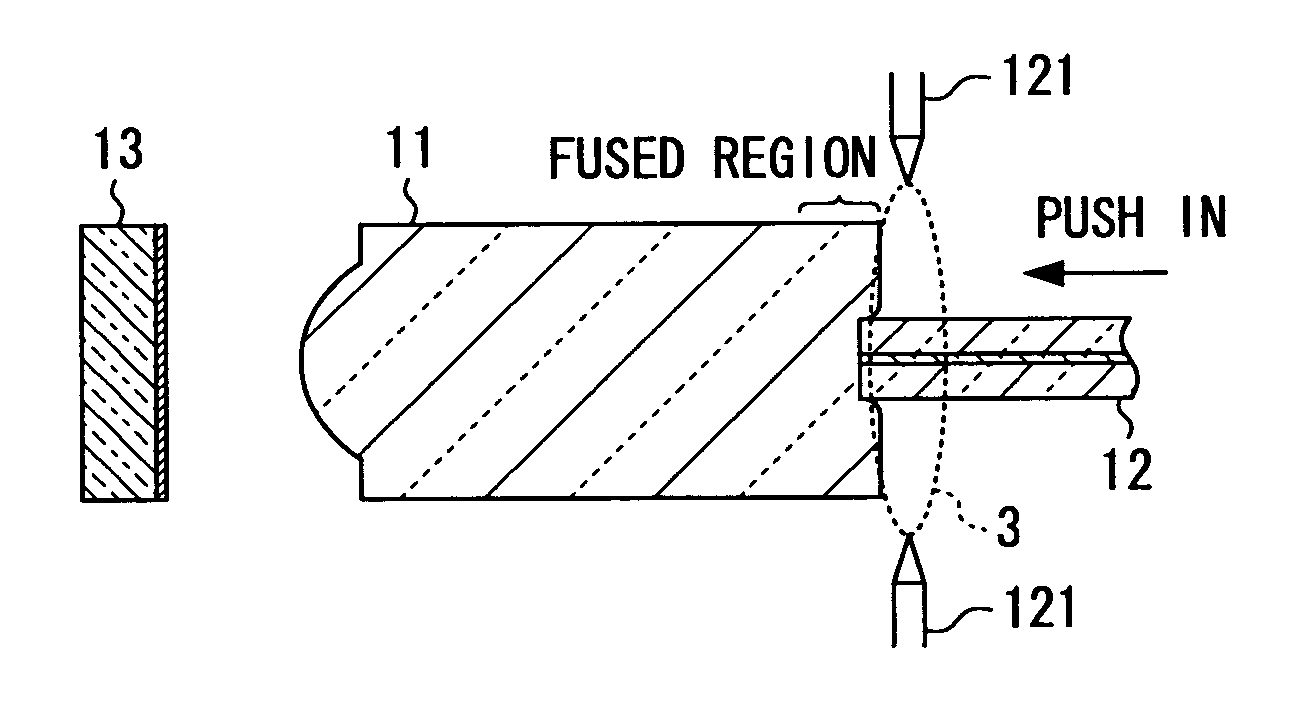
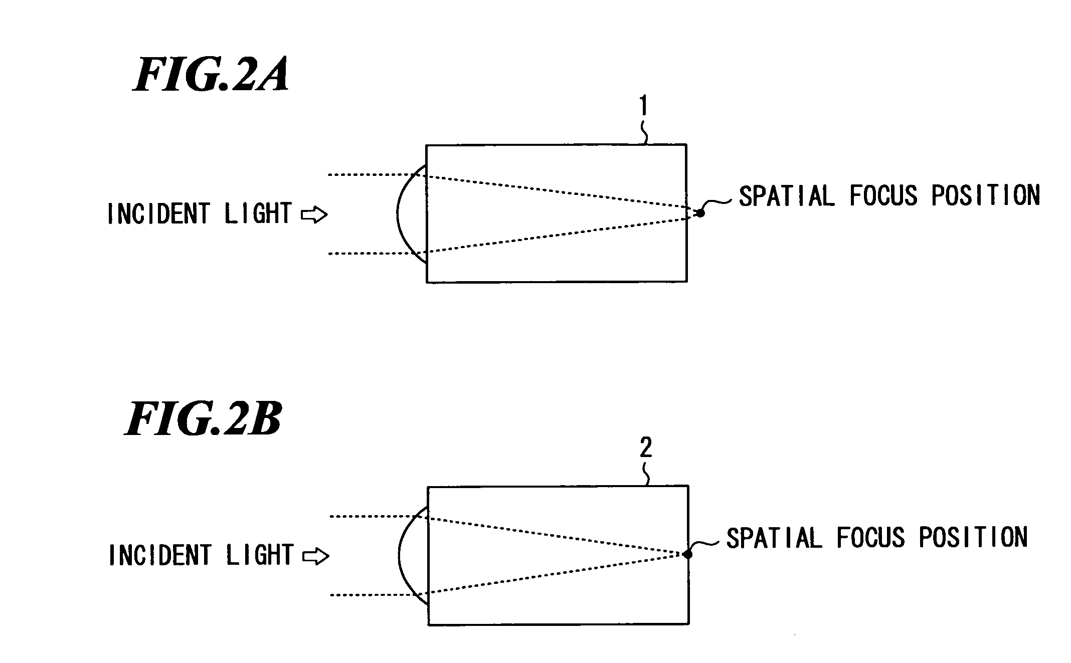
[0022] In addition, according to the present invention, the second optical device is pulled back after the second optical device is pushed into the first optical device, and therefore, it is possible to avoid the problem that the second optical device receives stress distortion and is damaged due to the contraction of the first optical device that has cooled down spontaneously. At that time, by using as the first optical device an optical device having a focus existing outside the end surface to which the second optical device is to be spliced, it is possible to accurately perform optical axis alignment of the first optical device and the second optical device, and it is possible to calculate the final splicing position of the second optical device relative to the first optical device based on the actually measured values. Accordingly, it is made possible to improve the precision of the third optical device. Further, even in the case where the front end of the second optical device misaligns from the optical axis due to the reaction force produced when the second optical device is pushed into the first optical device, the misalignment can be corrected by pulling back the second optical device.

Problems solved by technology

As described above, in the conventional fabrication method for fiber collimators, the number of devices to be used is large and processes required for fabrication are also complicated.
Further, since it takes such a long time as several minutes to 30 minutes to cure the adhesive, time for assembly is lengthened and the cost is increased.
Furthermore, since a resin adhesive is interposed between the lens and the optical fiber, an optical problem of distortion etc. of a plane of polarization, a problem of deviation of an optical axis that might be caused until the adhesive is cured, and a long-term problem of deterioration of the adhesive and so on arise.
Still further, in a lens used in such a fabrication method, a focus F thereof is normally set on the end surface 901a of the lens, and therefore, when light having high power is caused to enter an optical fiber, the light from the lens converges on a minute region at which the adhesive 905 is arranged, resulting in a problem that the spliced portion is easily damaged.
In such an optical waveguide device, although the problem caused by interposing a resin adhesive can be avoided, a third member (fused material) is used in addition to the optical waveguide and the optical fiber, and therefore, the fabrication process thereof is also complicated.
However, there arises another problem as follows in a fabrication method for fiber collimators by using the fused-splicing.
Further, since it is not possible to confirm the position of the focus F existing inside the lens before fused-splicing, it is difficult to precisely match the end surface 912a to the focus F when pushing the optical fiber 912 into the lens 911.
Therefore, the precision about Z-axis is also deteriorated.
Therefore, there also arises a problem that optical devices having high precision cannot be fabricated.

Method used


Image

  • Optical device and fabrication method and apparatus for the same
  • Optical device and fabrication method and apparatus for the same
  • Optical device and fabrication method and apparatus for the same

Examples


first embodiment

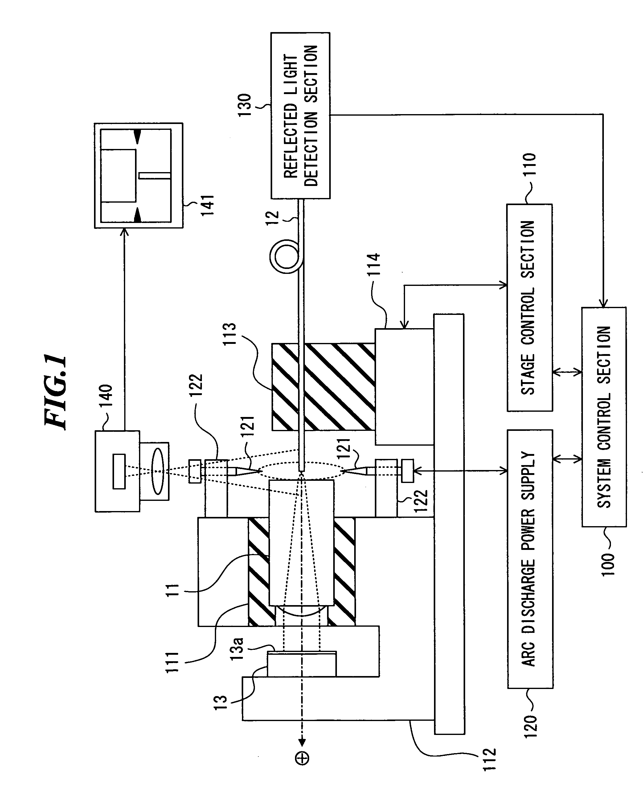
[0044]FIG. 1 is a schematic diagram showing a configuration of an optical device fabrication apparatus according to the present invention. The optical device fabrication apparatus is an apparatus for splicing a first optical device and a second optical device to fabricate a third optical device. In the present embodiment, a lens is used as the first optical device and an optical fiber is used as the second optical device, and thus a fiber collimator is fabricated.

[0045] The optical device fabrication apparatus shown in FIG. 1 includes a system control section 100, a stage control section 110, an arc discharge power supply 120, a reflected light detection section 130, a lens holder 111, a holder 112, a fiber holder 113, a movable stage 114, an arc electrode 121, and an arc electrode holder 122. Further, the optical device fabrication apparatus according to the present embodiment may also include a position observation section 140 and a monitor 141.

[0046] The system control section 1...

second embodiment

[0085] Next, an optical device fabrication apparatus according to the present invention will be described with reference to FIG. 8. The optical device fabrication apparatus shown in FIG. 8 is an apparatus for fabricating a multi-core fiber collimator in which a plurality of optical fibers are connected to one lens. In the present embodiment, the case where a two-core fiber collimator is fabricated will be described.

[0086] Instead of the fiber holder 113 and the reflected light detection section 130 shown in FIG. 1, a fiber holder 213 and a reflected light detection section 230 are provided, respectively. Other configurations are the same as those of the optical device fabrication apparatus shown in FIG. 1.

[0087] On the fiber holder 213, a groove such as V-groove or U-groove is formed for holding two optical fibers 22a and 22b to be connected to a lens 21 in close contact to each other or at a predetermined interval.

[0088]FIG. 9 is a diagram for describing a configuration of the re...

third embodiment

[0096] Next, an optical device fabrication apparatus according to the present invention will be described with reference to FIG. 11. The optical device fabrication apparatus shown in FIG. 11 is an apparatus for fabricating a facing module in which optical devices such as a translucent mirror or a wavelength selection mirror is arranged between two fiber collimators facing to each other. Such a facing module has functions of branching light, coupling light, dividing wavelength (WDW), etc. In the present embodiment, a facing module is fabricated, in which for light emitted from a light source and including two wavelength components of 1.3 μm and 1.55 μm, the wavelength component of 1.3 μm is reflected while the wavelength component of 1.55 μm is allowed to transmit by a wavelength selection mirror (a wavelength filter).

[0097] The optical device fabrication apparatus shown in FIG. 11 includes a system control section 300, a stage control section 310, an arc discharge power supply 320, ...


PUM


Abstract

An optical device fabrication method capable of fabricating optical devices with high precision and reliability in a simple process and at a low cost. The method of splicing a first optical device and a second optical device to fabricate a third optical device includes the steps of: (a) starting heating of an end surface of the first optical device to soften the end surface; (b) pushing the second optical device into the softened end surface to splice the first optical device and a joint surface of the second optical device to each other; (c) pulling back the second optical device to arrange the joint surface of the second optical device onto or outside of the end surface of the first optical device; and (d) terminating heating of the end surface to fix the first and second optical device spliced to each other.

Description

BACKGROUND OF THE INVENTION [0001] 1. Field of the Invention [0002] The present invention relates to an optical device to be used for transmitting light and a fabrication method and an apparatus for such an optical device. [0003] 2. Description of a Related Art [0004]FIGS. 17A-17C are diagrams for explaining a conventional fabrication method for fiber collimators. An end surface 901a of an aspheric lens 901 shown in FIG. 17A is flat-polished and coated with an anti-reflective film (AR coat) in order to reduce a reflection loss at a wavelength of light to be transmitted. On the other hand, an optical fiber 902 is inserted into a sleeve called as a capillary 903, which is precisely drilled, and fixed by an adhesive 904 such as resin. An end portion of the optical fiber 902 is cut together with the capillary 903, and an end surface 902a thereof is flat-polished and AR-coated. [0005] When splicing these two devices 901 and 902, as shown in FIG. 17B, an adhesive 905 such as resin is arra...

Claims


Application Information

Patent Timeline
IPC IPC(8): G02B6/32
CPCG02B6/2552G02B6/262G02B6/32G02B6/24
Inventor KOISHI, MUSUBU
Owner PRECISE GAUCO
Learn More