Manufacturing method of semiconductor device

a manufacturing method and semiconductor technology, applied in semiconductor devices, semiconductor/solid-state device details, electrical devices, etc., can solve problems such as film separation, interconnect delay, and reduction of interconnect capacitance, so as to prevent film separation, improve the adhesion of low dielectric film to the barrier metal, and improve the reliability of the damascene process

Inactive Publication Date: 2006-06-29
RENESAS ELECTRONICS CORP
View PDF1 Cites 30 Cited by
  • Summary
  • Abstract
  • Description
  • Claims
  • Application Information

AI Technical Summary

Benefits of technology

[0017] An object of the present invention is to provide a semiconductor device capable of improving adhesion of a low dielectric film having a bond of Si and a group made of organic constituents, such as MSQ, to a barrier metal at the interface in a damascene process and a manufacturing method thereof.
[0018] In particular, the object is to provide a structure of a semiconductor device capable of improving adhesion of the low dielectric interlayer film to an inorganic material, such as the barrier metal, by removing the organic constituents at the barrier metal / film interface, and a manufacturing method of the semiconductor device.
[0034] As has been described, according to the invention, in a damascene process using an insulation layer including a low dielectric film having a bond of Si and a group made of organic constituents, such as MSQ, provision of such a structure that can ensure adhesion between the low dielectric film and the barrier metal makes it possible to eliminate a problem that the barrier metal is separated during CMP and scratches are left on the low dielectric film, and to prevent film separation at the barrier metal / low dielectric film interface caused by stress resulted from the multi-level interconnection. The reliability of the damascene process using the low dielectric film can be thus improved.
[0035] Also, according to the invention, the plasma treatment is performed using a mixed gas of H2 and He, a He gas, etc. as a pre-step of depositing the barrier metal after the trench pattern or the via hole is formed in the insulation layer including a low dielectric film-having a bond of Si and a group made of organic constituents, such as MSQ. Thus, it is possible to replace the organic constituents (a methyl group in the case of MSQ) on the surface of the low dielectric film with hydrogen or decompose the organic constituents to form a dangling bond. Adhesion of the low dielectric film to the barrier metal can be thus improved. Consequently, it is possible to eliminate a problem that the barrier metal is separated during CMP and scratches are left on the low dielectric film, and to prevent film separation at the barrier metal / low dielectric film interface caused by stress resulted from the multi-level interconnection. The reliability of the damascene process using the low dielectric film can be thus improved.

Problems solved by technology

The damascene process can increase density of wiring patterns; however, when the wiring patterns are formed too close, a parasitic capacitance between the wiring patterns causes problematic interconnect delay.
Hence, a reduction in interconnect capacitance becomes an issue of great importance to improve the interconnect delay.
However, when a low dielectric film having a bond of Si and a group made of organic constituents, such as MSQ, is used as the second interlayer insulation film 18, it does not adhere well to an inorganic material, particularly, a barrier metal, and as shown in FIG. 3B, the barrier metal is separated from an MSQ-based low dielectric film during CMP, which gives rise to a problematic scratch 21 on the surface of the MSQ-based low dielectric film, or stress caused by the multi-level interconnection gives rise to problematic film separation 20 at the barrier metal / MSQ interface having poor adhesion.
This method, however, cannot avoid an increase in dielectric constant when a thick film is formed, and deterioration in adhesion associated with a pin-hole when a thin film is formed.
However, because merely a sputtered material is etched away through Ar sputtering, it proves to be ineffective in reforming the MSQ surface.
This method, however, has a problem that water comes into the film and a dielectric constant of the insulation film is increased; moreover, the surface of the film is made rough and a residue is left thereon.
However, the reliability reduced by poor adhesion of the low dielectric film to an inorganic material, particularly, a barrier metal, poses a serious problem, and there has been a need to develop a structure capable of increasing adhesion of the low dielectric film to the barrier metal, and a process capable of reforming the surface of the low dielectric film.

Method used


Image

  • Manufacturing method of semiconductor device
  • Manufacturing method of semiconductor device
  • Manufacturing method of semiconductor device

Examples


first example

[0081] Firstly, a dual damascene process according to a first example of the invention will be explained with reference to FIG. 7A through FIG. 9C. FIG. 7A through FIG. 9C are cross sections showing the step-by-step sequence of a via first process to which the structure and the plasma treatment of the invention are applied.

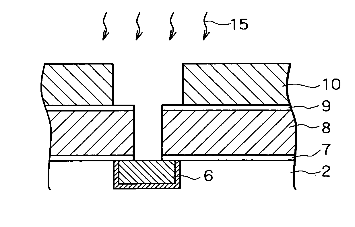
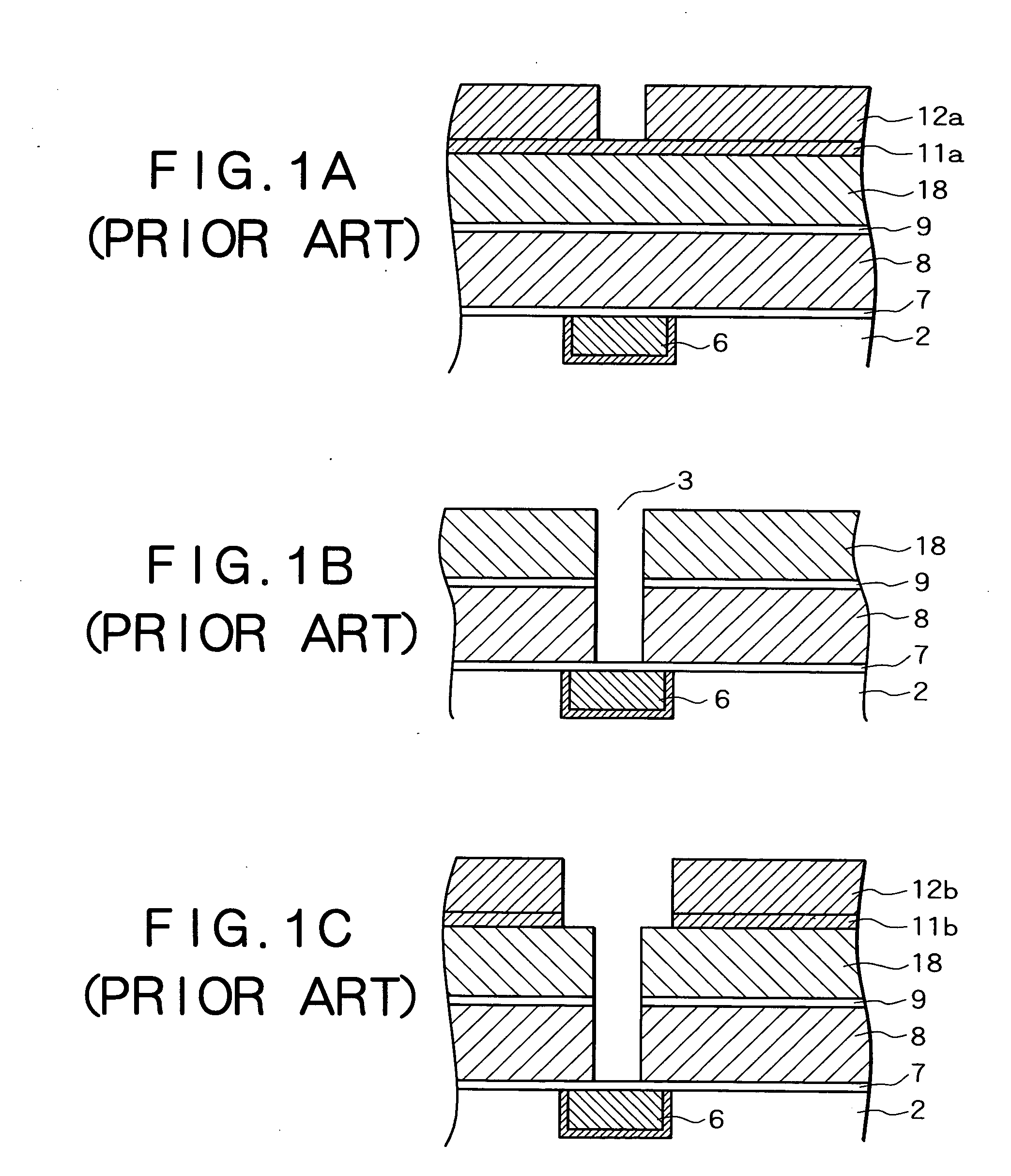
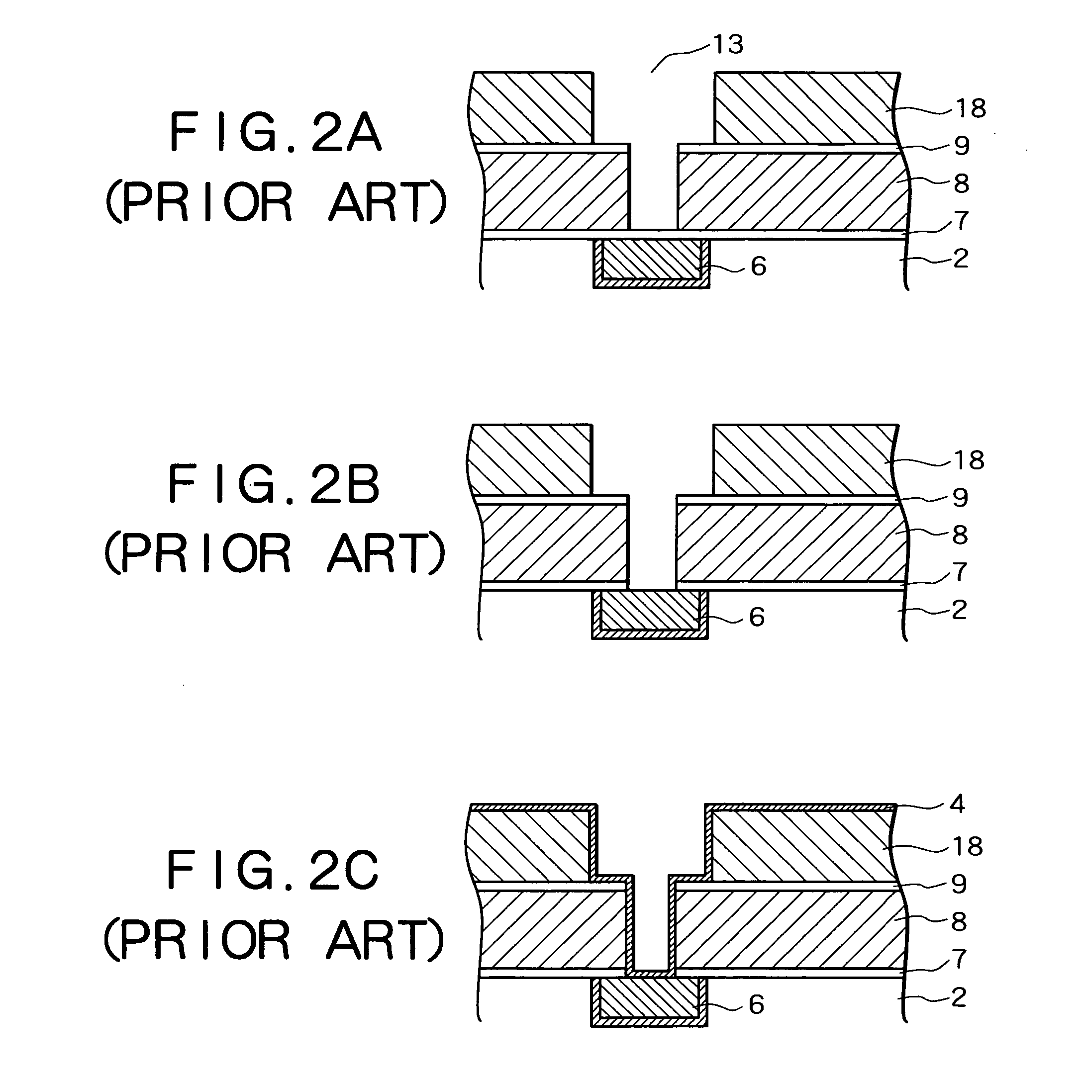
[0082] Initially, as shown in FIG. 7A, after a lower layer wiring 6 made of Cu, Cu alloy or the like is formed in a substrate 2 through a known method, a first etching stopper film 7, a first interlayer insulation film 8, a second etching stopper film 9, and a second interlayer insulation film 10 are formed sequentially from bottom to top in certain thickness through the CVD method, the plasma CVD method, etc. A film that can achieve the effect of the plasma treatment of the invention can be any low dielectric film containing hydrophobic groups having a large molecular structure like MSQ that contains methyl groups, and it may be MHSQ, SiC, SiCN, SiOC, SiCOH, etc...

second example

[0094] A dual damascene process according a second example of the invention will now be explained with reference to FIG. 10A through FIG. 13B. FIG. 10A through FIG. 13B are cross sections showing the step-by-step sequence of a dual hard mask process to which the structure and the plasma treatment of the invention are applied.

[0095] Initially, in the same manner as the first example above, as shown in FIG. 10A, after a lower layer wiring 6 made of Cu, Cu alloy or the like is formed in a substrate 2 through a known method, a first etching stopper film 7, a first interlayer insulation film 8, a second etching stopper film 9, and a second interlayer insulation film 10 are formed sequentially from bottom to top through the CVD method, the plasma CVD method, etc. Then, in this example, a first hard mask film 16 and a second hard mask film 17 to be used as an etching mask for a wiring trench pattern are deposited on these films.

[0096] This example will also describe a case where MSQ is u...

third example

[0108] A single damascene process according to a third example of the invention will now be explained with reference to FIG. 14A through FIG. 17C. FIG. 14A through FIG. 17C are cross sections showing the step-by-step sequence of the single damascene process to which the structure and the plasma treatment of the invention are applied.

[0109] Initially, as shown in FIG. 14A, a first etching stopper film 7 and a first interlayer insulation film 8 are formed sequentially from bottom to top in certain thickness atop a lower layer wiring 6 through the CVD method, the plasma CVD method, etc. Then, after a first reflection preventing film 11a to be used to control reflection of exposing light is deposited on the first interlayer insulation film 8 in a thickness of approximately 50 nm, chemically amplified resist to be used to form a via hole pattern is applied thereon in a thickness of approximately 500 nm, which is subjected to exposure and development through ArF photolithography. A first...


PUM

PropertyMeasurementUnit
poweraaaaaaaaaa
thicknessaaaaaaaaaa
thicknessaaaaaaaaaa

Abstract

A manufacturing method of a semiconductor device including a step of forming a via hole in an insulation layer including an organic low dielectric film, such as MSQ, SiC, and SiCN, and then embedding a wiring material in the via hole through a barrier metal. According to this method, a plasma treatment is performed after the via hole is formed and before the barrier metal is deposited, using a He / H2 gas capable of replacing groups (methyl groups) made of organic constituents and covering the surface of the exposed organic low dielectric film (MSQ) with hydrogen, or a He gas capable decomposing the groups (methyl groups) without removing organic low dielectric molecules. As a result, the surface of the low dielectric film (MSQ) is reformed to be hydrophilic and adhesion to the barrier metal is hence improved, thereby making it possible to prevent the occurrence of separation of the barrier metal and scratches.

Description

BACKGROUND OF THE INVENTION [0001] 1. Field of the Invention [0002] The present invention relates to a structure of a semiconductor device and a manufacturing method thereof, and more particularly to, in a damascene process using a low dielectric film having a bond of Si and a group made of organic constituents, such as MSQ, an interface structure of a barrier metal and the low dielectric film and a surface treatment method thereof. [0003] 2. Description of the Related Art [0004] To meet the high integration of a semiconductor device and a reduction in chip size in recent years, not only the miniaturization of the wiring, but also the multi-level interconnection is being promoted. As a method of forming a multi-level interconnect structure, a so-called damascene process is generally performed, by which an interconnect is formed by embedding Cu in both a via hole and a wiring trench pattern concurrently followed by planarization through the CMP (Chemical Mechanical Polishing) method....

Claims


Application Information

Patent Timeline
Patent Type & Authority Applications(United States)
IPC IPC(8): H01L21/4763H01L21/3205H01L21/768H01L23/532
CPCH01L21/32051H01L21/76802H01L21/76807H01L21/76811H01L21/76814H01L23/53295H01L21/76831H01L21/76843H01L23/53238H01L23/5329H01L21/76826H01L2924/0002H01L2924/00H01L21/28
Inventor TONEGAWA, TAKASHIARITA, KOJIUSAMI, TATSUYAMORITA, NOBORUOHTO, KOICHISASAKI, YOICHIOHNISHI, SADAYUKIKITAO, RYOHEI
Owner RENESAS ELECTRONICS CORP
Why Eureka
Try Eureka