Image sensor

Active Publication Date: 2006-07-06
MARVELL ASIA PTE LTD +1
View PDF9 Cites 13 Cited by
  • Summary
  • Abstract
  • Description
  • Claims
  • Application Information

AI Technical Summary

Benefits of technology

[0009] An advantage of the present invention is to provide an image sensor, which prevents the generation of a reddish effect in an output image.
[0010] An advantage of the present invention is to provide an image sensor, which enables a decrease in light concentration so that a uniform image can be obtained with a desired dynamic range.
[0011] Additional features and advantages of the invention will be set forth in the description which follows, and will be apparent from the description, or may be learned by practice of the invention. The objectives and other advantages of the invention will be realized and attained by the structure particularly pointed out in the written description and claims hereof as well as the appended drawings.
[0012] To achieve these and other advantages and in accordance with the purpose of the invention, as embodied and broadly described, an image sensor includes a color filter array including separate color filters for respectively filtering light according to wavelength, wherein the separate color filters include a long-wavelength filter, and a plurality of microlenses respectively formed on the separate color filters of the color filter array, the microlenses corresponding to the long-wavelength filter and having relative sizes differing according to disposition with respect to the color filter array.
[0013] In another aspect of the present invention, an image sensor includes a s

Problems solved by technology

Increase of the fill factor is limited, however, by the presence of the associated logic and signal processing circuitry of each photodiode.
This refractivity

Method used


Image

  • Image sensor
  • Image sensor
  • Image sensor

Examples


Embodiment Construction

[0023] Reference will now be made in detail to exemplary embodiments of the present invention, examples of which are illustrated in the accompanying drawings. Wherever possible, like reference designations will be used throughout the drawings to refer to the same or similar parts.

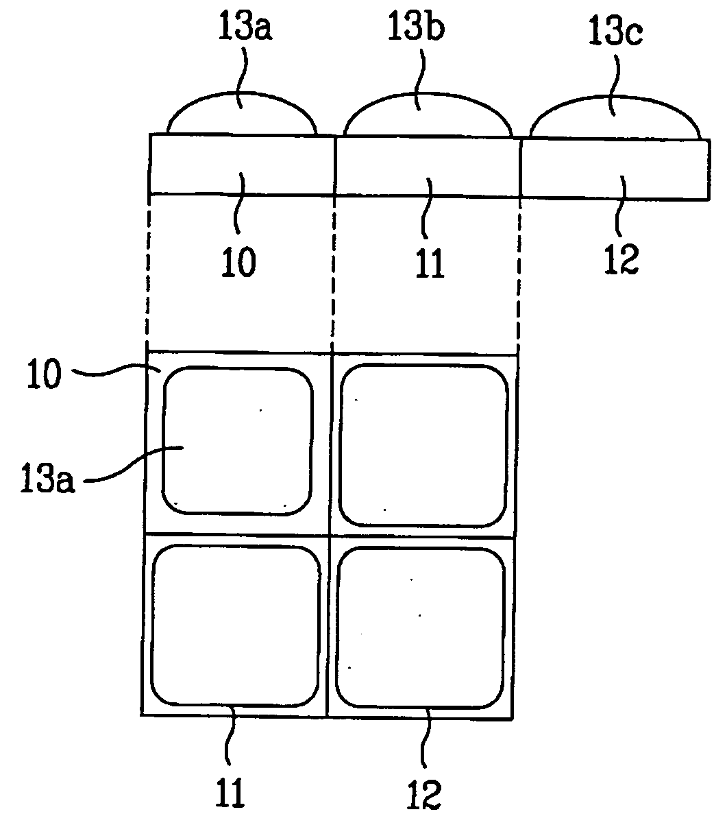
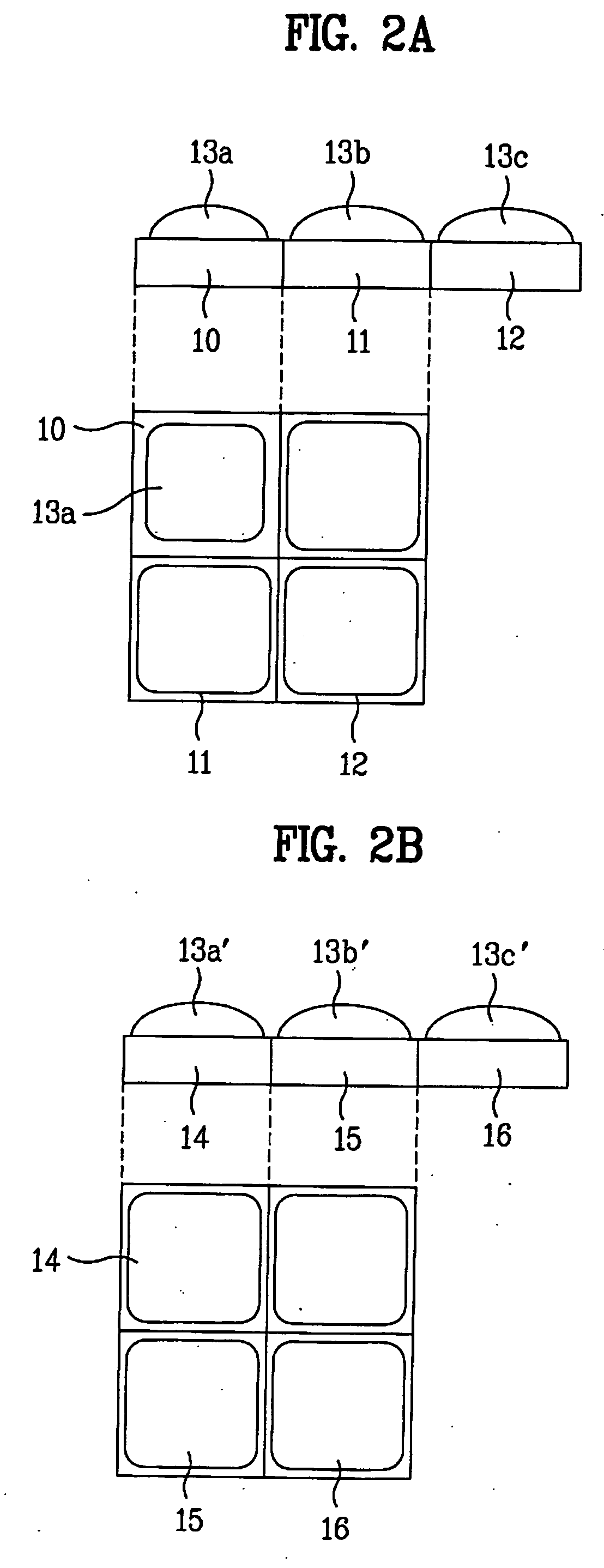
[0024] An image sensor according to the present invention includes a plurality of photosensors, for example, photodiodes, for receiving red light, green light, and blue light, formed on a semiconductor substrate having a central image region and a peripheral image region. An insulating interlayer, a patterned metal layer, and a passivation layer may be formed on the photosensors. A color filter array is formed on the passivation layer, and a plurality of microlenses are formed on the color filter array. The color filter array and microlenses are formed, using CMOS technology, across the central image region and the peripheral image region of the semiconductor substrate, as shown in FIGS. 2A and 2B.

[0025] ...


PUM


Abstract

A image sensor has a plurality of microlens disposed across an image area in which centrally disposed red pixels are provided with smaller microlenses and peripherally disposed red pixels are provided with larger microlenses. The size differential, which amounts to a small percentage to compensate for a refractivity differential per wavelength of incident light across the image area, prevents the generation of a reddish effect in an output image. The image sensor includes a color filter array having separate color filters including a long-wavelength filter, and a plurality of microlenses respectively formed on the separate color filters, wherein the microlenses corresponding to the long-wavelength filter have relative sizes differing according to disposition with respect to the color filter array.

Description

[0001] This application claims the benefit of Korean Patent Application No. 1.0-2004-0117227, filed on Dec. 30, 2004, which is hereby incorporated by reference for all purposes as if fully set forth herein. BACKGROUND OF THE INVENTION [0002] 1. Field of the Invention [0003] The present invention relates to an image sensor, and more particularly, to an image sensor that prevents the generation of a reddish effect in an output image. [0004] 2. Discussion of the Related Art [0005] Image sensors are semiconductor devices for converting an optical image to an electrical signal and include CMOS image sensors having a number of metal-oxide-semiconductor (MOS) transistors, corresponding to the number of pixels, integrated on a single chip with peripheral circuitry. The circuitry sequentially outputs the electrical signals of the MOS transistors. CMOS image sensors use complimentary MOS technology to decrease feature size, power consumption, and fabrication costs and are applicable to such p...

Claims


Application Information

Patent Timeline
IPC IPC(8): H01L27/00
CPCH01L27/14603H01L27/14621H01L27/14625H01L27/14627H01L27/14645H01L27/146
Inventor KIM, SANG SIK
Owner MARVELL ASIA PTE LTD
Why Eureka
Try Eureka