TFT array substrate and fabrication method thereof

Inactive Publication Date: 2006-07-06
LG DISPLAY CO LTD
View PDF9 Cites 61 Cited by
  • Summary
  • Abstract
  • Description
  • Claims
  • Application Information

AI Technical Summary

Benefits of technology

[0043] An advantage of the present invention is to provide a TFT array substrate and a fabrication method thereof, which can protect TFTs without a passivation layer and reduce the manufacturing cost and the number of the required masks.
[0044] Another advantage of the present invention is to provide a TFT array substrate and a fabrication method thereof, which can prevent galvanic corrosion due to opening of a data pad by forming the data pad in a jumping structure of a gate metal pattern and a data metal pattern.
[0045] A further another advantage of the present invention is to provide a TFT array substrate and a fabrication method thereof, which can reduce the number of the required processes by separating even/odd data lines to form a static electricity prevention structure.
[0046] Additional advantages, objects, and features of the invention will be set forth in part in the description which follows and in part will become apparent to those having ordinary skill in the art upon examination of the following or may be learned from practice of the invention. The objectives and other advantages of the invention may be realized and attained by the structure particularly pointed out in the written description and claims hereof as well as the appended drawings.
[0047] To achieve these objects and other advantages and in accordance with the purpose of the invention, as embodied and broadly described herein, there is provided a TFT array substrate including: a gate electrode connected to a gate line; a source electrode connected to a data line, the data line crossing the gate line to define a pixel region; a drain electrode facing the source electrode wi

Problems solved by technology

In the LCD, because fabrication of the TFT array substrate requires a semiconductor process and a plurality of mask processes, the manufacturing process thereof is complicated and thus manufacturing costs increase.
Because the PECVD apparatus, the spin coating apparatus, or the spinless

Method used


Image

  • TFT array substrate and fabrication method thereof
  • TFT array substrate and fabrication method thereof
  • TFT array substrate and fabrication method thereof

Examples


Example

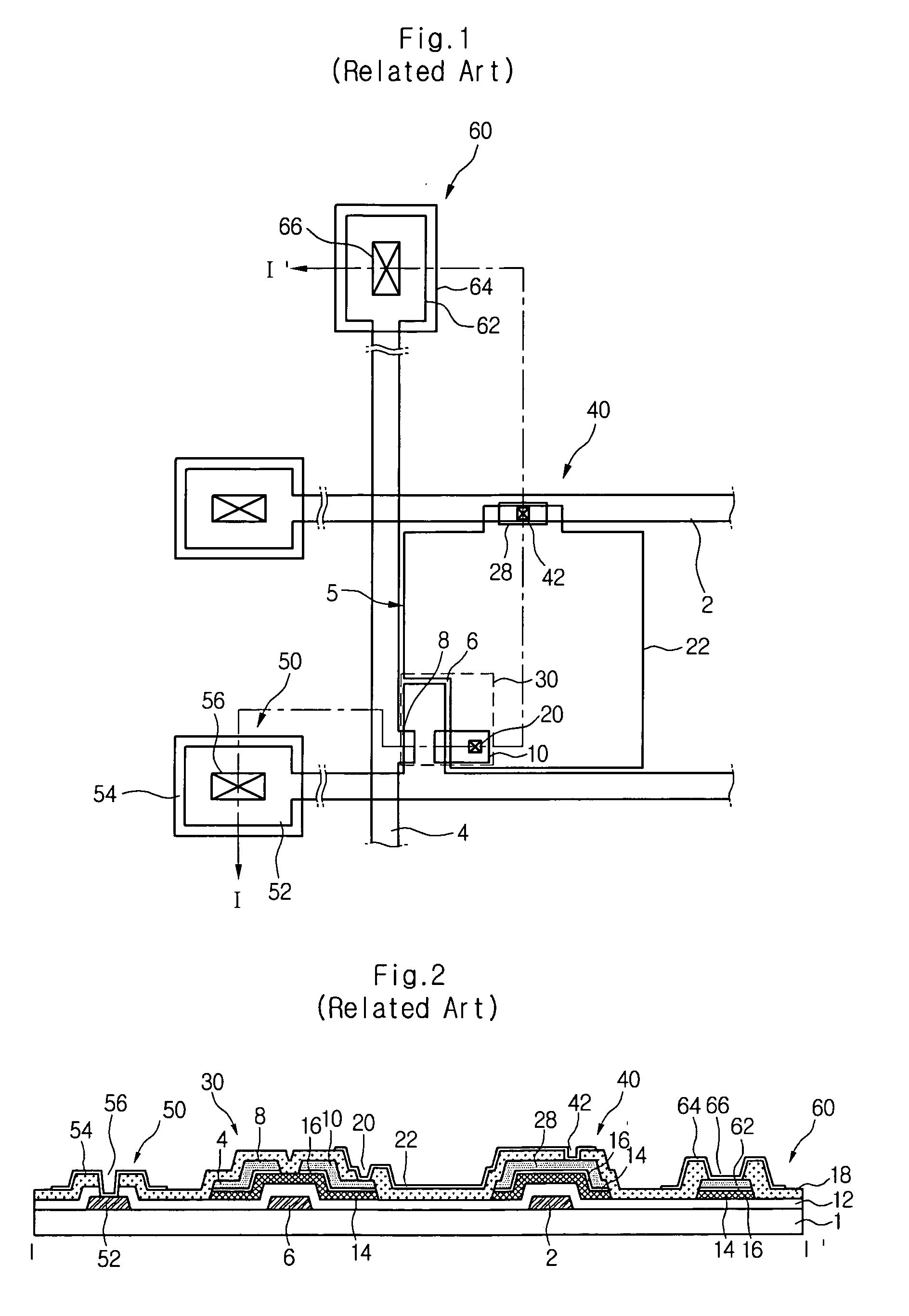
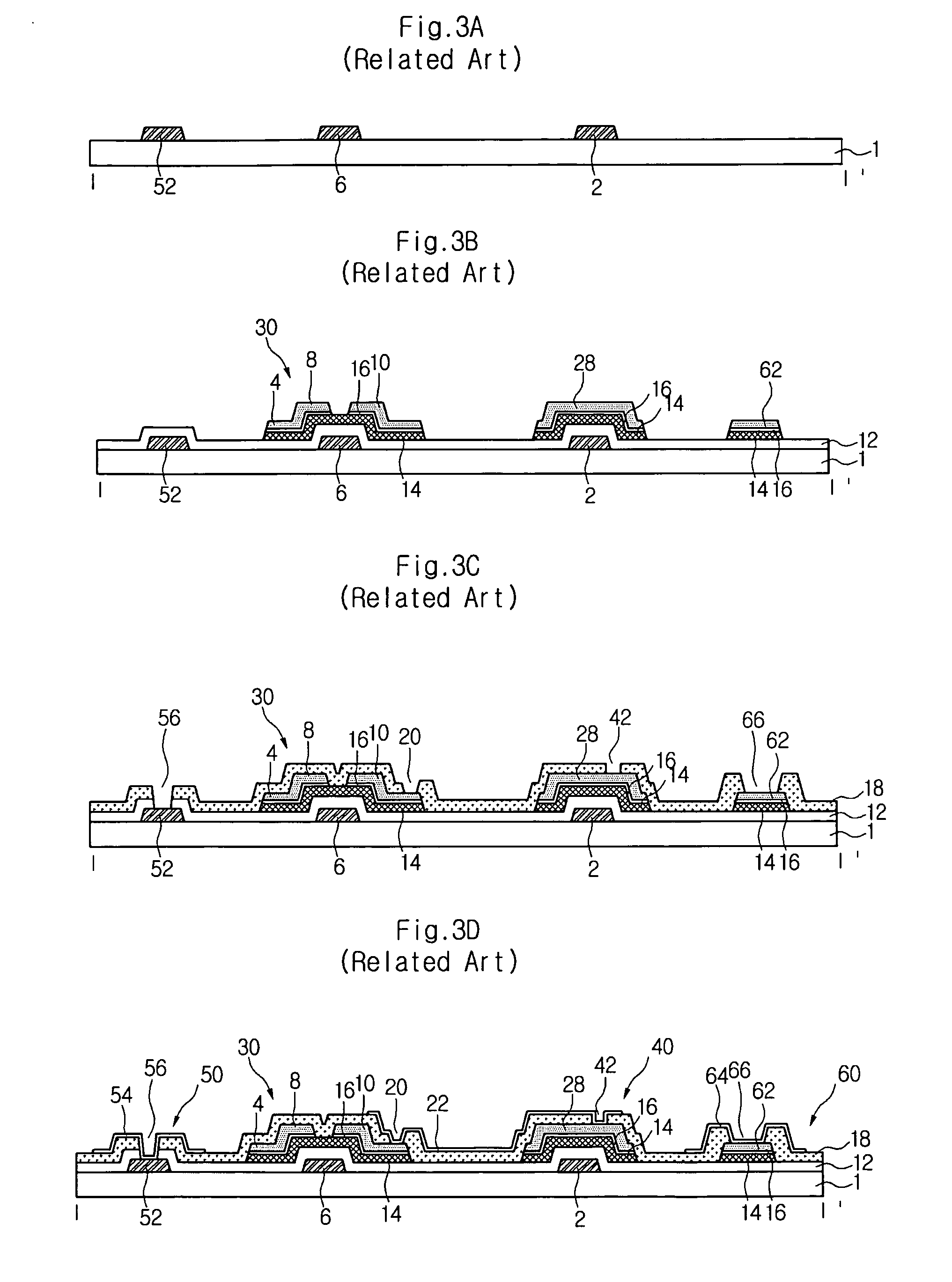
[0064] Reference will now be made in detail to the preferred embodiments of the present invention, examples of which are illustrated in the accompanying drawings.

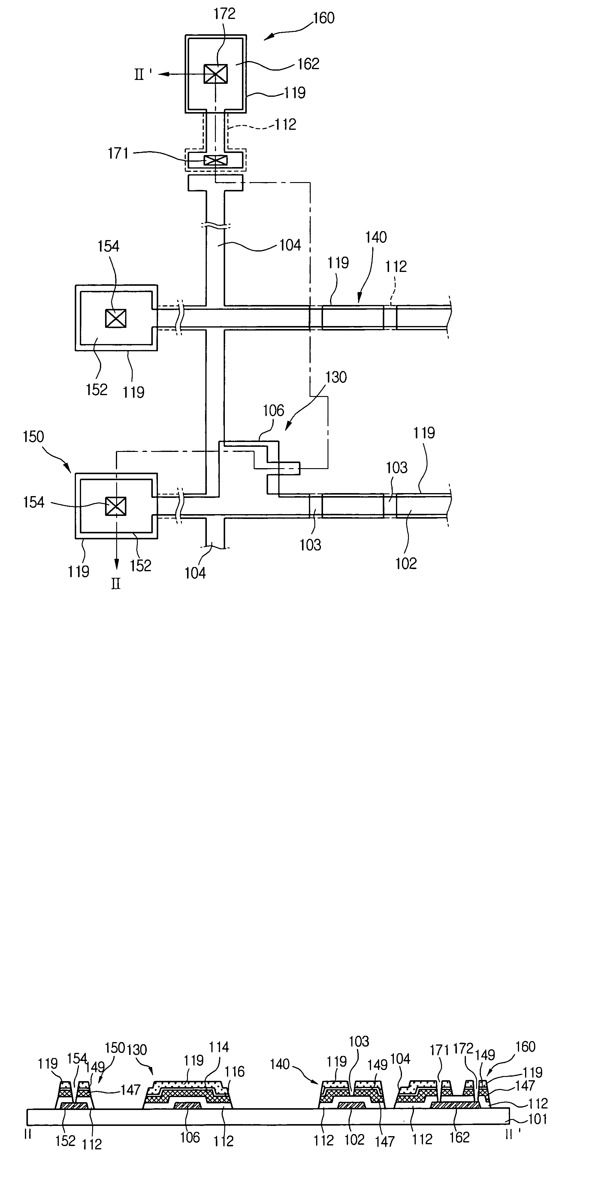
[0065]FIG. 4 is a plan view of a TFT array substrate according to the present invention, and FIG. 5 is a sectional view taken along line II-II′ of FIG. 4.

[0066] Referring to FIGS. 4 and 5, the TFT array substrate includes a gate insulating layer 112 on a lower substrate 101, a TFT 130 formed at each crossing portion, a pixel electrode 122 formed in a pixel region 105 defined by the crossing gate and data lines, and a channel passivation layer 120 for protecting the TFT 130.

[0067] Also, the TFT array substrate further includes a storage capacitor 140 formed by an overlapping portion of the gate line 102 and the pixel electrode 122, a gate pad 150 connected to the gate line 102, and a data pad 160 connected to the data line 104 by a jumping structure. The gate line 102 that supplies a gate signal and the data line 104 that...


PUM


Abstract

A TFT array substrate is provided. The TFT array substrate includes a gate electrode connected to a gate line; a source electrode connected to a data line, the data line crossing the gate line to define a pixel region; a drain electrode facing the source electrode with a channel interposed therebetween; a semiconductor layer forming the channel between the source electrode and the drain electrode; a channel passivation layer formed on the channel to protect the semiconductor layer; a pixel electrode disposed in the pixel region to contact with the drain electrode; a storage capacitor including the pixel electrode extending over the gate line to form a storage area on a gate insulating layer on which a semiconductor layer pattern and a metal layer pattern are stacked; a gate pad extending from the gate line; and a data pad connected to the data line.

Description

[0001] This application claims the benefit of Korean Patent Application No. 117243 / 2004, filed on Dec. 30, 2004, which is hereby incorporated by reference for all purposes as if fully set forth herein. BACKGROUND OF THE INVENTION [0002] 1. Field of the Invention [0003] The present invention relates to a thin film transistor (TFT) array substrate, and more particularly, to a TFT array substrate and a fabrication method thereof capable of protecting TFTs without a passivation layer and preventing galvanic corrosion of a data or gate pad. [0004] 2. Discussion of the Related Art [0005] A liquid crystal display (LCD) displays an image by controlling the light transmittance of liquid crystal (LC) using an electric field. [0006] The LCD drives the LC using an electric field generated between a pixel electrode and a common electrode respectively disposed on an upper substrate and a lower substrate facing each other. [0007] The LCD has a TFT array substrate (lower array substrate) and a colo...

Claims


Application Information

Patent Timeline
IPC IPC(8): H01L29/76
CPCG02F1/13458G02F1/136213H01L27/124H01L27/1255H01L27/1288G02F1/136
Inventor CHOI, YOUNGYU, HONGCHO, KILEE, JAEJUNG, BO
Owner LG DISPLAY CO LTD
Why Eureka
Try Eureka