Flip chip contact (FCC) power package
a power package and chip technology, applied in the field of semiconductor devices, can solve the problems of imposing limitations on the miniaturization of electronic devices, package occupying several times the area of the ic chip, and the cost of conventional chip packaging is relatively high
- Summary
- Abstract
- Description
- Claims
- Application Information
AI Technical Summary
Benefits of technology
Problems solved by technology
Method used
Image

Examples
Embodiment Construction
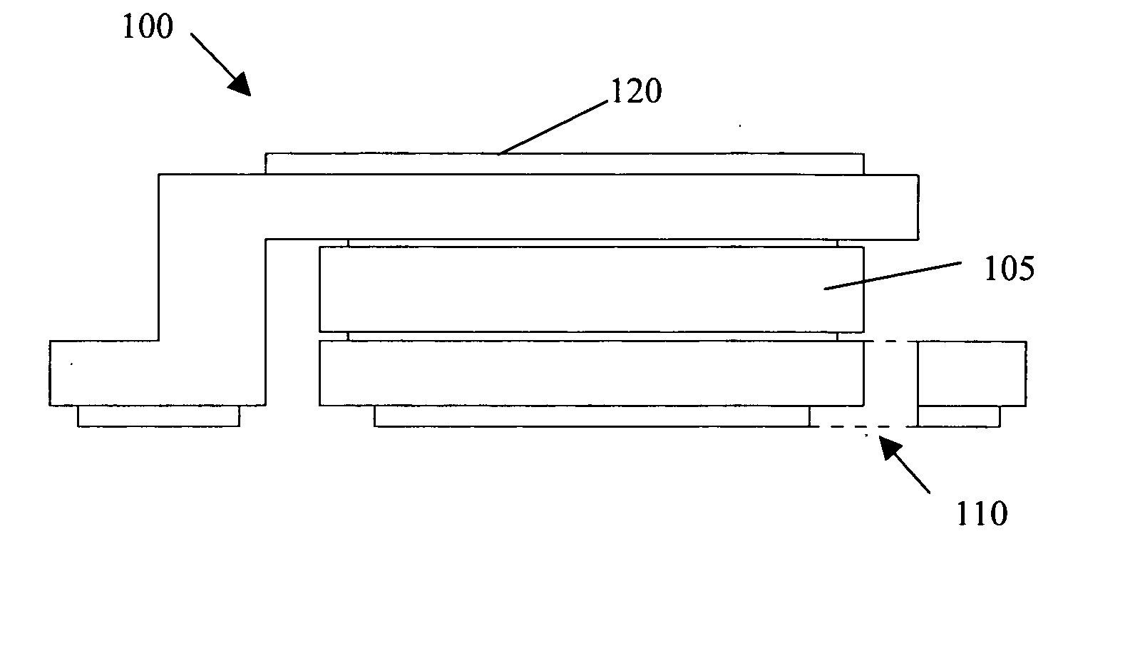
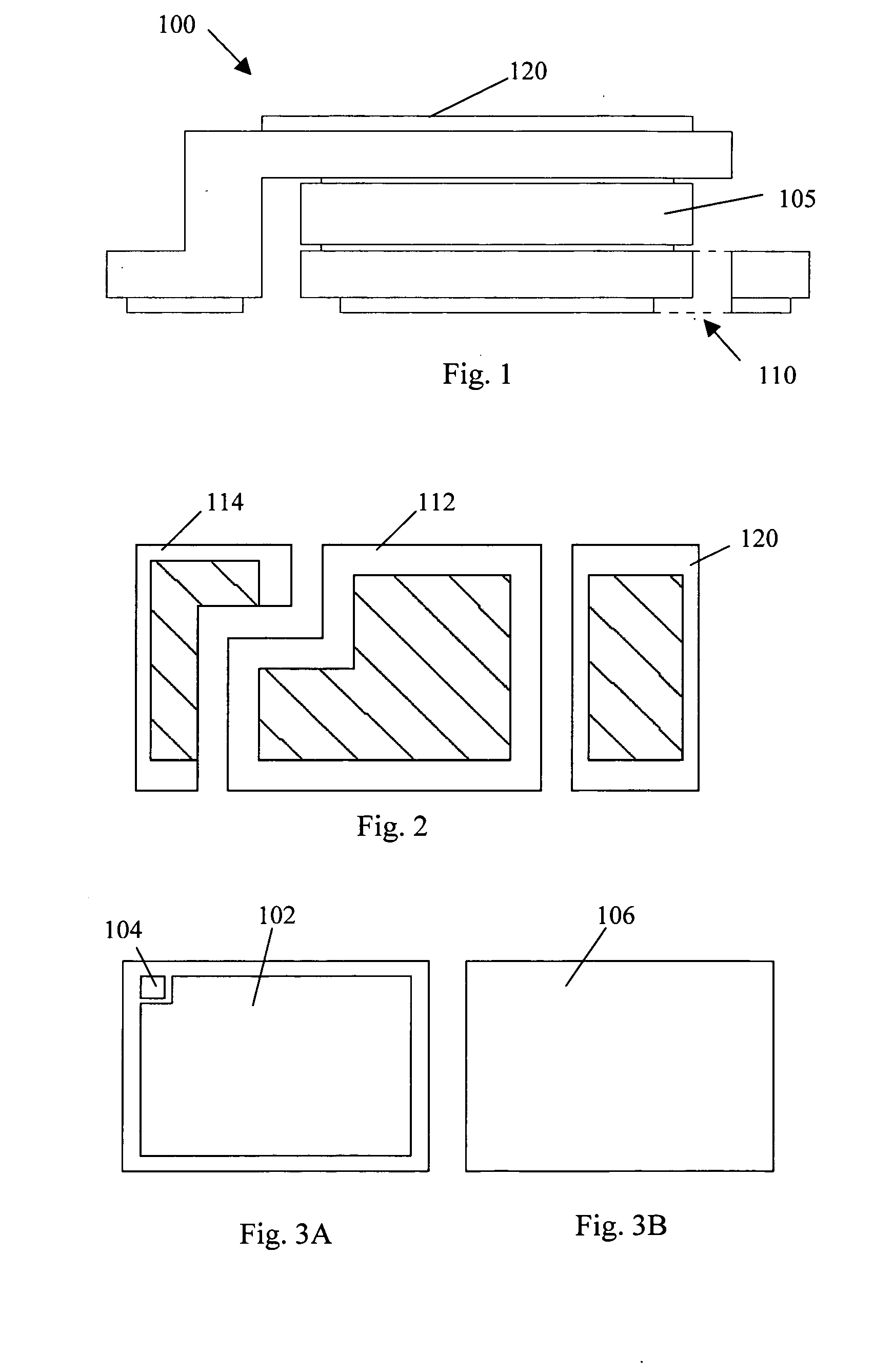
[0020] Referring to FIG. 1 for a side cross sectional view of a package 100 for a semiconductor device, e.g., a MOSFET device. The structure of the package 100 includes an IC chip, i.e., a die 105, flips on an electrically conducting lead frame 110. The lead frame is a conducting frame composed of frame plated with Al, Cu, Ag, and Ni or may be any electrically conducting frame. Unlike conventional flip chip configurations, the flip chip 105 is connecting to the lead frame 110 without requiring a prior process to form “bumps” on the IC chip as interconnect. For a MOSFET package, the package 100 comprises three layers. A top conducting-frame 120 is connected to drain of the MOSFET. The MOSFET chip 105 is disposed between the top layer and the bottom layer. The bottom conducting-frame 110 is connected to source and gate of the MOSFET.
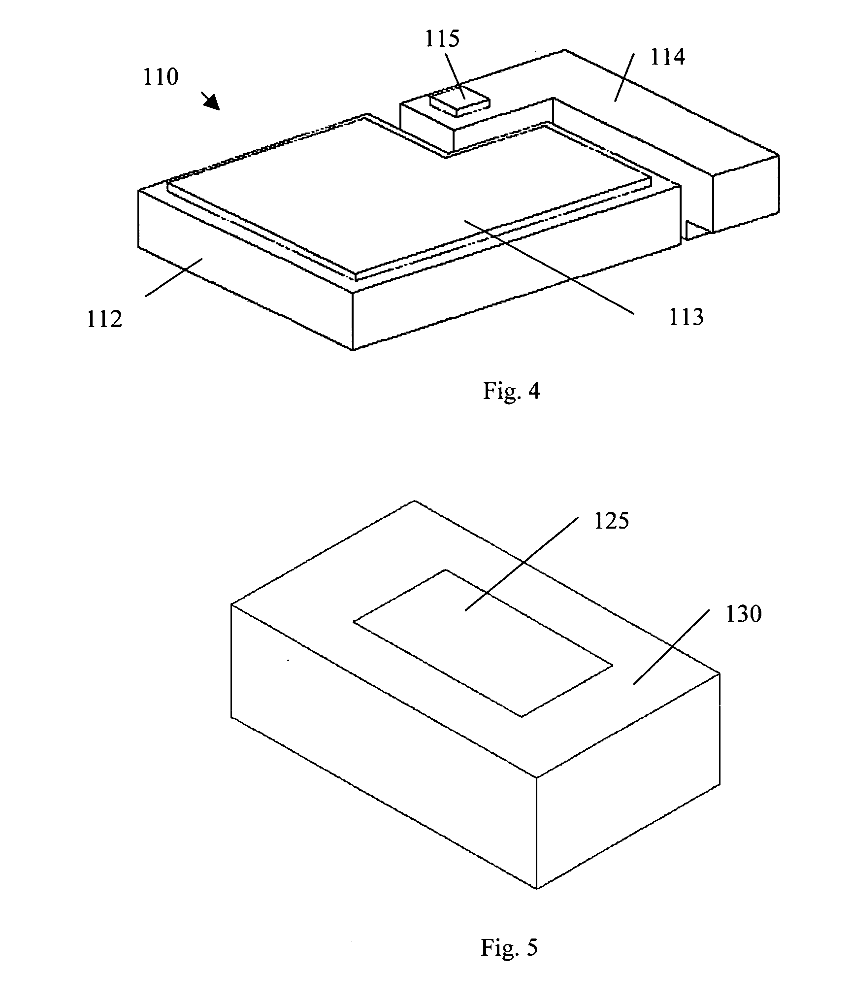
[0021]FIG. 2 shows the bottom view of the device. The bottom-conducting frame 110 is divided into a source portion 112 and a gate portion 114. When the d...
PUM
 Abstract
Description
Claims
Application Information
 - Generate Ideas
- Intellectual Property
- Life Sciences
- Materials
- Tech Scout
- Unparalleled Data Quality
- Higher Quality Content
- 60% Fewer Hallucinations
Browse by: Latest US Patents, China's latest patents, Technical Efficacy Thesaurus, Application Domain, Technology Topic, Popular Technical Reports.
© 2025 PatSnap. All rights reserved.Legal|Privacy policy|Modern Slavery Act Transparency Statement|Sitemap|About US| Contact US: help@patsnap.com