Memory device and method for manufacturing the same

a memory device and memory technology, applied in semiconductor devices, digital storage, instruments, etc., can solve the problems of difficult to reduce the area of the cell, the cell threshold may be shifted, and the cell can be wiped excessively, so as to reduce the programming voltage, reduce the cell size, and reduce the programming voltage.

Inactive Publication Date: 2006-07-06
DONGBU ELECTRONICS CO LTD
View PDF8 Cites 7 Cited by
  • Summary
  • Abstract
  • Description
  • Claims
  • Application Information

AI Technical Summary

Benefits of technology

[0013] An object of the present invention is to provide a split gate (flash) EEPROM cell and a method for manufacturing the same, in which a control gate and a floating gate have a vertical structure (e.g., a height greater than the width), to minimize the cell size and / or to obtain a high coupling ratio, thereby lowering a programming voltage.

Problems solved by technology

In this case, even though an area of the cell is relatively small, it may have a problem in that the erase function of the cell can be excessive.
In such an excessive erase problem, the cell threshold may be shifted after many repeated write / erase cycles.
However, the control gate 5 is formed not only on the floating gate 3 but also over the p-type semiconductor substrate 1, so that it can be difficult to decrease the area of the cell (or make it about the same size as the stacked gate structure).
As a result, it may be difficult to satisfy the trend toward high integration in semiconductor devices containing EEPROM cells, particularly flash EEPROM cells.

Method used


Image

  • Memory device and method for manufacturing the same
  • Memory device and method for manufacturing the same
  • Memory device and method for manufacturing the same

Examples


first embodiment

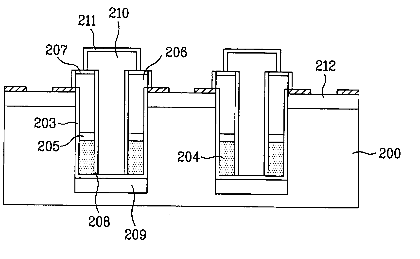
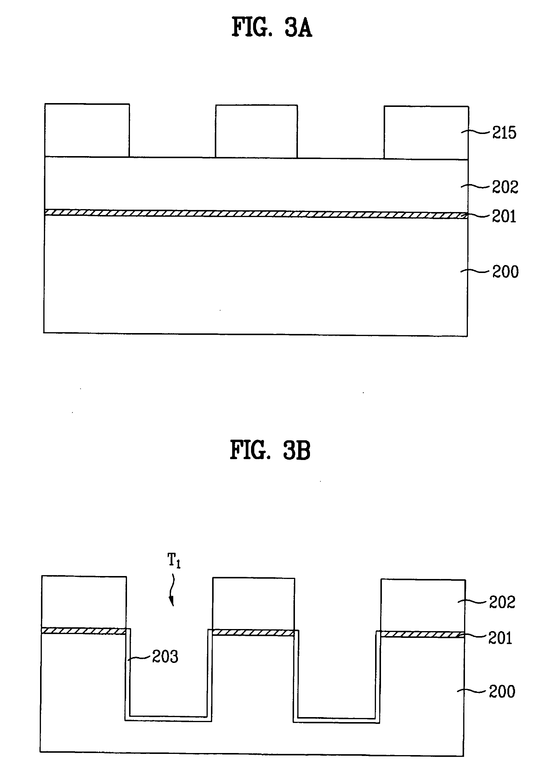
[0029]FIG. 3A to FIG. 3G are cross sectional views of the process for manufacturing a split gate flash EEPROM cell according to the present invention.

[0030] As shown in FIG. 3A, a semiconductor substrate 200 may have therein an active area and a field area, defined at least in part by a device isolation layer (not shown). Then, a buffer oxide (e.g., silicon dioxide) layer 201 and an insulating layer 202 are sequentially deposited on the semiconductor substrate 200. After that, a first photoresist 215 is coated on the insulating layer 202, and then the first photoresist 215 is patterned on the insulating layer 202 by a conventional photolithography (e.g., exposure and development) process. At this time, the insulating layer 202 may comprise a nitride layer (e.g., silicon nitride).

[0031] As shown in FIG. 3B, the insulating layer 202, the buffer oxide layer 201 and the semiconductor substrate 200 are etched to a predetermined depth (e.g., a trench depth) using the patterned first phot...

second embodiment

[0041]FIG. 4A to FIG. 4G are cross-sectional views of an exemplary process for fabricating a split gate (flash) EEPROM cell according to the present invention.

[0042] As shown in FIG. 4A, a semiconductor substrate 300 generally contains an active area and a field area, defined at least in part by a device isolation layer (not shown). In this state, a buffer oxide layer 301 and an insulating layer 302 are sequentially deposited on the semiconductor substrate 300. Then, a first photoresist 315 is coated on the insulating layer 302, and the first photoresist 315 is patterned by a conventional photolithography (e.g., exposure and development) process. As for insulating layer 202 (e.g., FIG. 3A), the insulating layer 302 may comprise a nitride layer.

[0043] Referring to FIG. 4B, the insulating layer 302, the buffer oxide layer 301 and the semiconductor substrate 300 are etched to a predetermined depth by using the patterned first photoresist 315 as a mask, thereby forming a trench T1 in a...


PUM


Abstract

A split gate (flash) EEPROM cell and a method for manufacturing the same is disclosed, in which a control gate and a floating gate are formed in a vertical structure, to minimize a size of the cell, to obtain a high coupling ratio, and to lower a programming voltage. The split gate EEPROM cell includes a semiconductor substrate having a trench; a tunneling oxide layer at sidewalls of the trench; a floating gate, a dielectric layer and a control gate in sequence on the tunneling oxide layer; a buffer dielectric layer at sidewalls of the floating gate and the control gate; a source junction in the semiconductor substrate at the bottom surface of the trench; a source electrode in the trench between opposing buffer dielectric layers, electrically connected to the source junction; and a drain junction on the surface of the semiconductor substrate outside the trench.

Description

[0001] This application claims the benefit of Korean Application No. P2004-118276, filed on Dec. 31, 2004, which is hereby incorporated herein by reference in its entirety. BACKGROUND OF THE INVENTION [0002] 1. Field of the Invention [0003] The present invention relates to a memory device, and more particularly, to a Split Gate (Flash) Electrically Erasable Programmable Read Only Memory (EEPROM) and a method for manufacturing the same. [0004] 2. Discussion of the Related Art [0005] A typical example of a nonvolatile memory device, which has electric program and erase functions, is a (flash) EEPROM (Electrically Erasable Programmable Read Only Memory) cell. Such (flash) EEPROM cells may be classified into a stack structure and a split gate structure. [0006]FIG. 1 shows a cross sectional view of a stack type EEPROM cell according to the related art. FIG. 2 shows a cross sectional view of a split gate type EEPROM cell according to the related art. [0007] As shown in FIG. 1, the stack t...

Claims


Application Information

Patent Timeline
Patent Type & Authority Applications(United States)
IPC IPC(8): G11C8/02
CPCH01L21/823807H01L21/823878H01L21/84H01L27/1203H01L29/0847H01L29/1054H01L29/66575H01L29/78Y10S438/938
Inventor KIM, HEUNG JIN
Owner DONGBU ELECTRONICS CO LTD
Why Eureka
Try Eureka