Wavelength-division-multiplexed passive optical network

a passive optical network and wavelength division technology, applied in the field of active-type semiconductor optical devices, can solve the problems of limited wavelength of erbium-doped optical fiber amplifiers, high fabrication costs and large volume, and largely limited in the selection of wavelength bands and ranges. , to achieve the effect of removing the polarization dependence of ligh

Inactive Publication Date: 2006-07-06
SAMSUNG ELECTRONICS CO LTD
View PDF5 Cites 5 Cited by
  • Summary
  • Abstract
  • Description
  • Claims
  • Application Information

AI Technical Summary

Benefits of technology

[0008] Accordingly, the present invention has been made to solve the above-mentioned problems occurring in the prior art and provides additional advantages, by providing e a broadband light source capable of eliminating a polarization dependence of light having a broad wavelength band generated from a semiconductor optical active device.

Problems solved by technology

However, the erbium-doped optical fiber amplifier has limited wavelengths and has a problem in that it has high fabrication costs and large volume.
The erbium-doped optical fiber amplifier stably generates a high-power polarization-insensitive light, but is largely limited in selection of a wavelength band and range as compared with the semiconductor optical active device.
In contrast, the semiconductor optical active device has advantages in that the wavelength band and range can be simply selected and miniaturization is possible, but has drawbacks in that it has relatively poor characteristics in output, polarization, and spectrum.
However, a light generated from the semiconductor optical active device has a large polarization dependence, which limits the application in an optical communication network.
However, it is practically impossible to precisely control the polarization mode of light, and also it is impossible to completely eliminate all polarization dependence without causing a decrease in the yield of products due to inherent characteristic of the semiconductor devices.

Method used


Image

  • Wavelength-division-multiplexed passive optical network
  • Wavelength-division-multiplexed passive optical network
  • Wavelength-division-multiplexed passive optical network

Examples


first embodiment

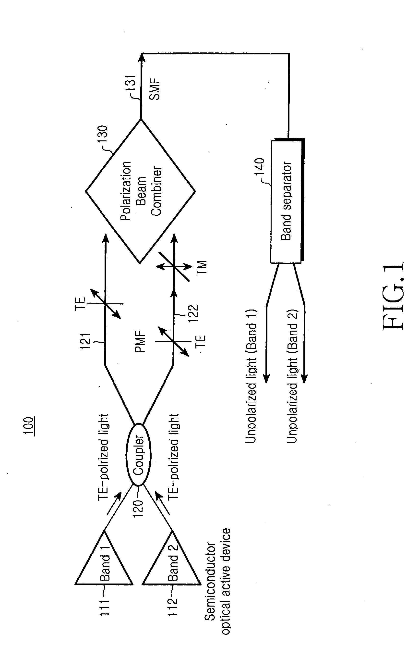
[0015]FIG. 1 is a block diagram illustrating the configuration of a broadband light source according to the present invention.

[0016] As shown, the broadband light source 100 includes two or more semiconductor optical active devices 111 and 112, an optical coupler 120, first and second optical lines 121 and 122, a polarization beam combiner 130, a band separator 140, and a single-mode optical fiber 131. The single-mode optical fiber 131 is located between the polarization beam combiner 130 and the band separator 140 and transmits a polarization-independent light to the band separator 140.

[0017] The semiconductor optical active devices 111 and 112 may include a superluminescent diode (SLD), a semiconductor optical amplifier (SOA), or other equivalent optical device capble of generating a light of a specific polarization mode. The semiconductor optical active devices 111 and 112 generate TE polarized lights having wavelength bands different from each other.

[0018] The optical coupler ...

second embodiment

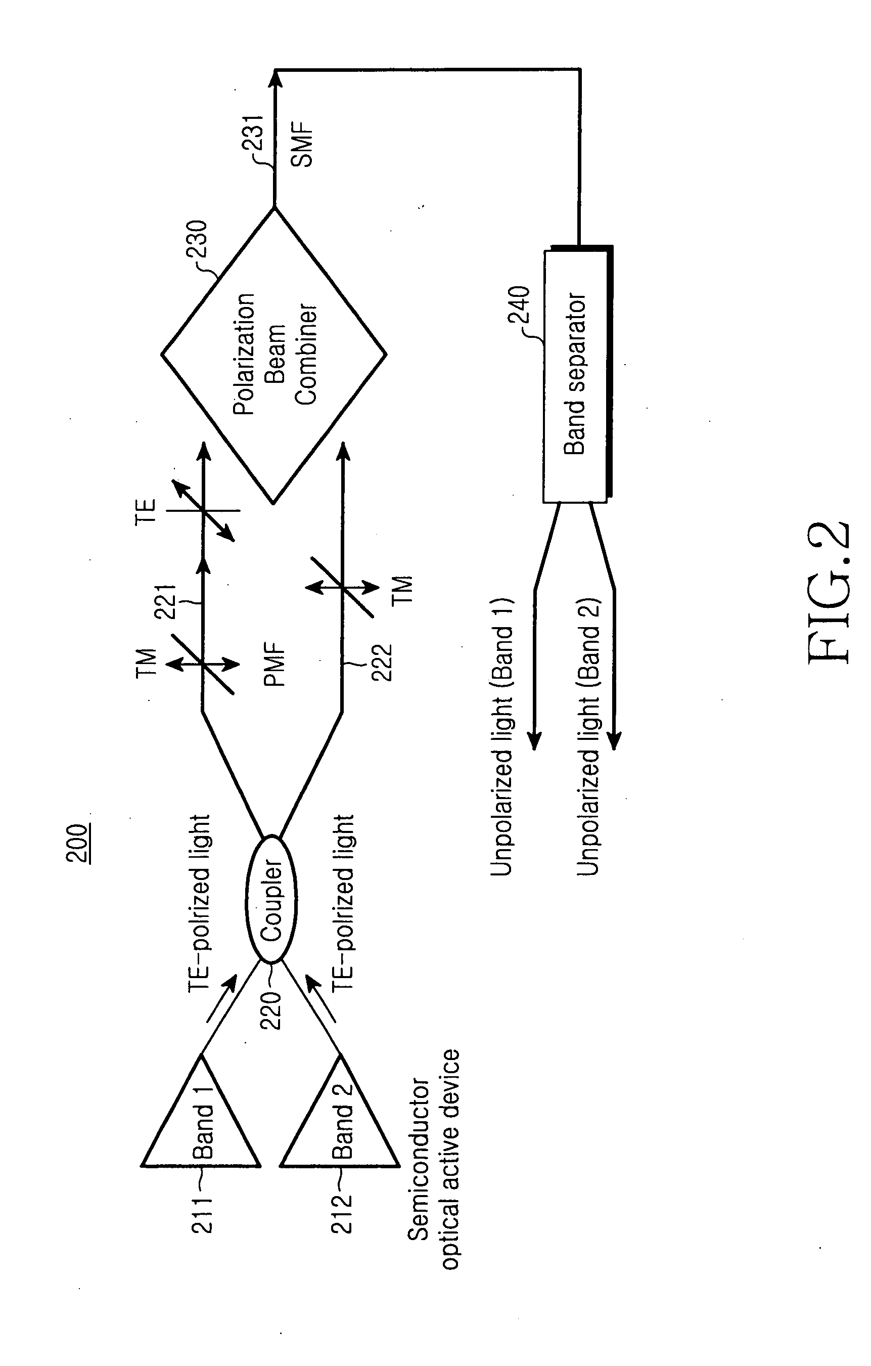
[0022]FIG. 2 is a block diagram illustrating the configuration of a broadband light source according to the present invention.

[0023] As shown, the broadband light source 200 includes two or more semiconductor optical active devices 211 and 212, an optical coupler 220, first and second optical lines 221 and 222, a polarization beam combiner 230, a band separator 240, and a single-mode optical fiber 231. The single-mode optical fiber 231 is located between the polarization beam combiner 230 and the band separator 240, and transmits a polarization-independent light to the band separator 240.

[0024] The semiconductor optical active devices 211 and 212 generate TM polarized lights having wavelength bands different from each other and output the generated TM polarized lights to the optical coupler 220. The optical coupler 220 divides each of the TM polarized lights into two TM polarized lights, then outputs the two divided TM polarized lights (including a first TM polarized light and a se...

third embodiment

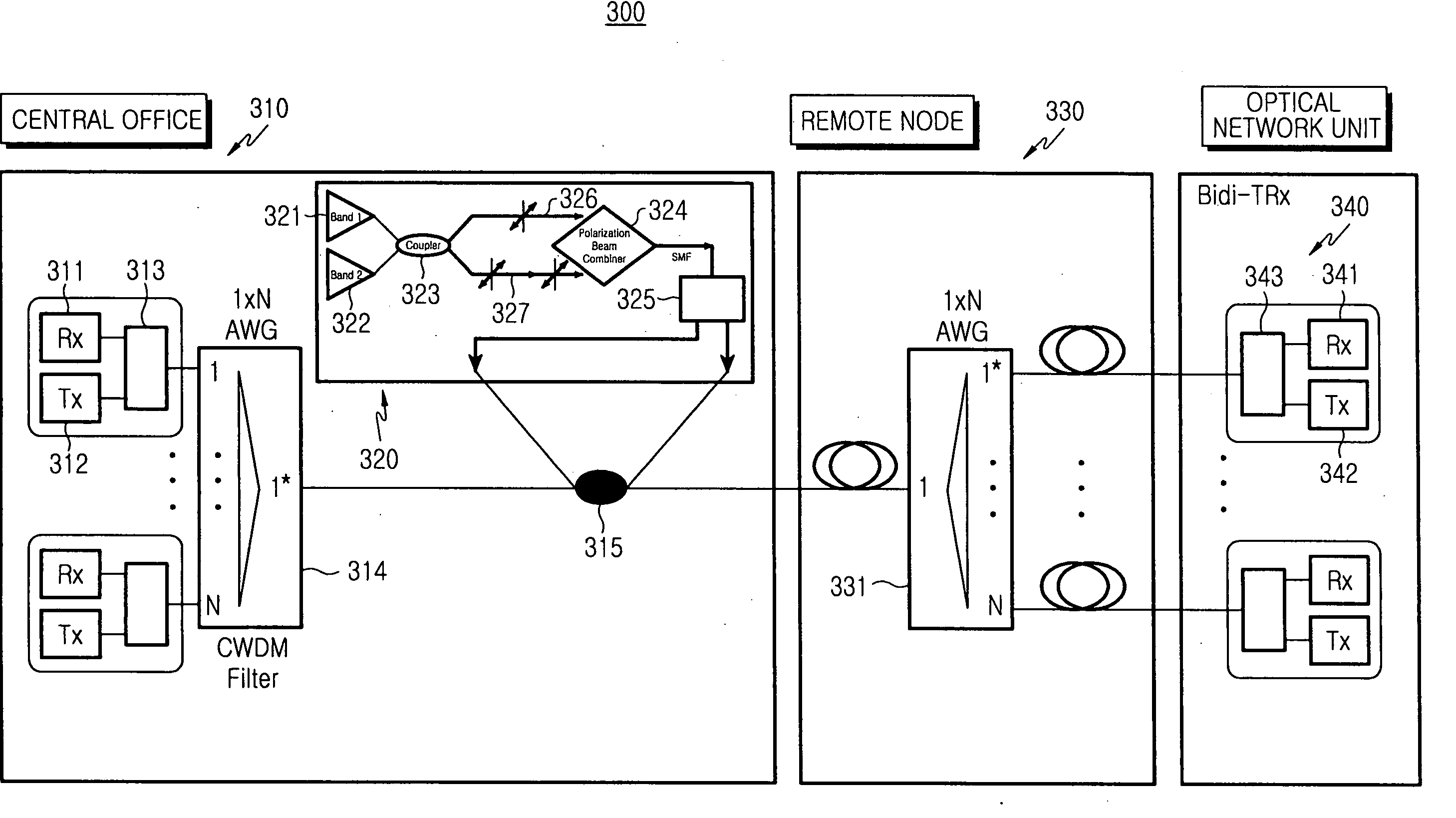
[0027]FIG. 3 is a block diagram illustrating a passive optical network including a broadband light source according to the present invention. The passive optical network 300 includes a central office 310, a plurality of optical network units 340, and a remote node 330 located between the central office 310 and the optical network units 340. The central office 310 generates wavelength-locked downstream optical signals and also detects upstream optical signals, and each of the optical network units 340 receives a downstream optical signal of a relevant wavelength. The remote node 330 and the central office 310 are linked by a main optical fiber, and each of the optical network units 340 is linked to the remote node 330 by a local optical fiber.

[0028] The central office 310 includes a broadband light source 320, a plurality of downstream light sources 312, a plurality of upstream optical detectors 311, a plurality of wavelength selection combiners 313, a multiplexer / demultiplexer 314, ...


PUM


Abstract

A broadband light source includes: at least two semiconductor optical active devices for generating TE polarized lights of different wavelength bands; an optical coupler for dividing each of the TE polarized lights input from each of the semiconductor optical active devices into two TE polarized lights, and outputting the two TE polarized lights, the two TE polarized lights including a first TE polarized light and a second TE polarized light; a first optical line for transmitting the first TE polarized light, while maintaining a polarization mode of the first TE polarized light; a second optical line for converting the second TE polarized light into a TM polarized light; a polarization beam combiner for combining the first TE polarized light and the TM polarized light to generate a polarization-independent light; and a band separator for separating and outputting the polarization-independent light according to wavelength bands.

Description

CLAIM OF PRIORITY [0001] This application claims to the benefit under 35 U.S.C. 119 of an application entitled “Wavelength-Division-Multiplexed Passive Optical Network,” filed in the Korean Intellectual Property Office on Jan. 3, 2005 and assigned Serial No. 2005-111, the entire contents of which are incorporated herein by reference. BACKGROUND OF THE INVENTION [0002] 1. Field of the Invention [0003] The present invention relates to a semiconductor optical device, and more particularly to an active-type semiconductor optical device capable of generating a broad wavelength band light. [0004] 2. Description of the Related Art [0005] In general, broadband light sources capable of generating a broad band light include an erbium-doped optical fiber amplifier and a semiconductor optical active device which may be used to generate wavelength-locked optical signals in a wavelength-division-multiplexed optical network or may be used as a spectrum-sliced light source. In the wavelength-divisi...

Claims


Application Information

Patent Timeline
Patent Type & Authority Applications(United States)
IPC IPC(8): H04J14/00H01L33/00H04B10/25H04B10/27H04B10/272H04J14/02
CPCH04J14/02H04J14/0226H04J14/0282H04J14/06H04J14/0246H04J14/025H04B10/00G02B6/27H04B10/25H04L12/28
Inventor KIM, SEUNG-WOOLEE, JEONG-SEOKHWANG, SEONG-TAEK
Owner SAMSUNG ELECTRONICS CO LTD
Why Eureka
Try Eureka