Aqueous cleaner with low metal etch rate

a cleaner and low metal etching technology, applied in the direction of anionic surface active compounds, chemistry apparatus and processes, detergent compositions, etc., can solve the problems of contaminant layer, insufficient cleaning of surface containing copper, and contamination of semiconductor substrate surfaces

Inactive Publication Date: 2006-07-06
ADVANCED TECH MATERIALS INC
View PDF11 Cites 37 Cited by
  • Summary
  • Abstract
  • Description
  • Claims
  • Application Information

AI Technical Summary

Benefits of technology

[0016] In one aspect the present invention is a cleaning solution for cleaning copper-containing microelectronic substrates comprises 0.122 to 0.155 wt % tetramethylammonium hydroxide, 0.22 to 3.48 wt % monoethanolamine, 0.084 to 1.36 wt % gallic acid, balance deionized water. The pH of the solution should be greater than 10.
[0017] In another aspect the present invention is a post-CMP cleaning solution for cleaning microelectronic substrates comprising 1.0 to 1.5 wt % of a concentrate inserting essentially of tetramethylammonium hydroxide in an amount in the range from about 8.0 wt % to about 12.4 wt %, monoethanolamine in an amount in the range from about 14.4 wt % to about 27.8 wt %, gallic acid in an amount in the range from about 5.6 wt % to about 10.9 wt %, balance deionized water; and 98.5 to 99 wt % deionized water.
[0018] In yet another aspect the present invention is a cleaning composition wherein a concentrate containing 8.0 wt % to 12.4 wt % TMAH, 14.9 to 27.8 wt % MEA, 5.6 to 10.9 wt % gallic acid, balance deionized water is diluted (mixed) in a ratio of 1 part concentrate to between 100 and 150 parts deionized water that can be used in a static bath or a bath agitated ultrasonically to effectuate post-CMP cleaning.
[0019] In still another embodiment the present invention is a cleaning composition consisting essentially of 0.033 to 0.140 wt % TMAH, 0.06 to 0.30 wt % MEA, 0.013 to 0.07 wt % corrosion inhibitor selected from the group consisting of gallic acid, ascorbic acid and mixtures thereof, balance deionized water.

Problems solved by technology

The CMP process, however, leaves contamination on the surfaces of the semiconductor substrate.
In addition, the contaminant layer may comprise reaction products of the polishing slurry and the polished surfaces.
Conventional post-CMP processes are inadequate for cleaning surfaces containing copper.

Method used


Image

  • Aqueous cleaner with low metal etch rate
  • Aqueous cleaner with low metal etch rate
  • Aqueous cleaner with low metal etch rate

Examples


Embodiment Construction

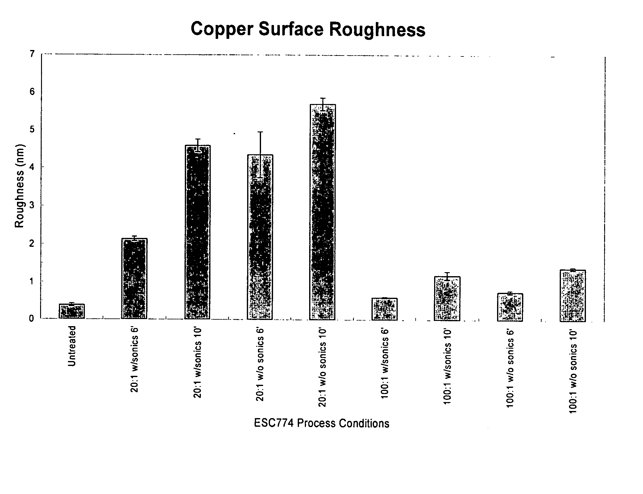
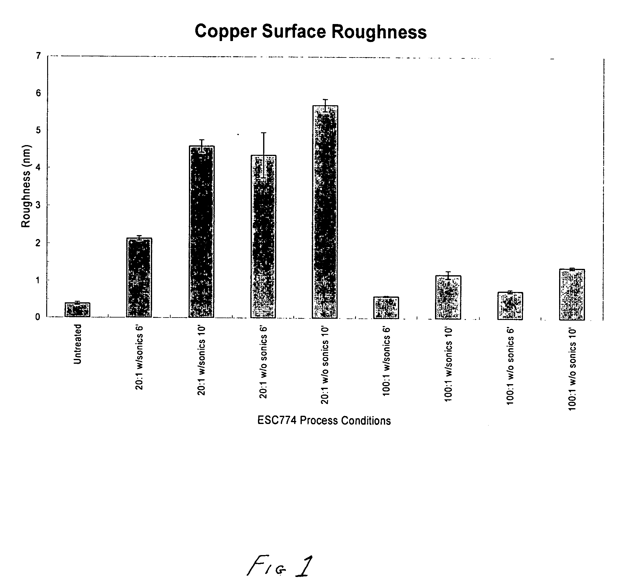
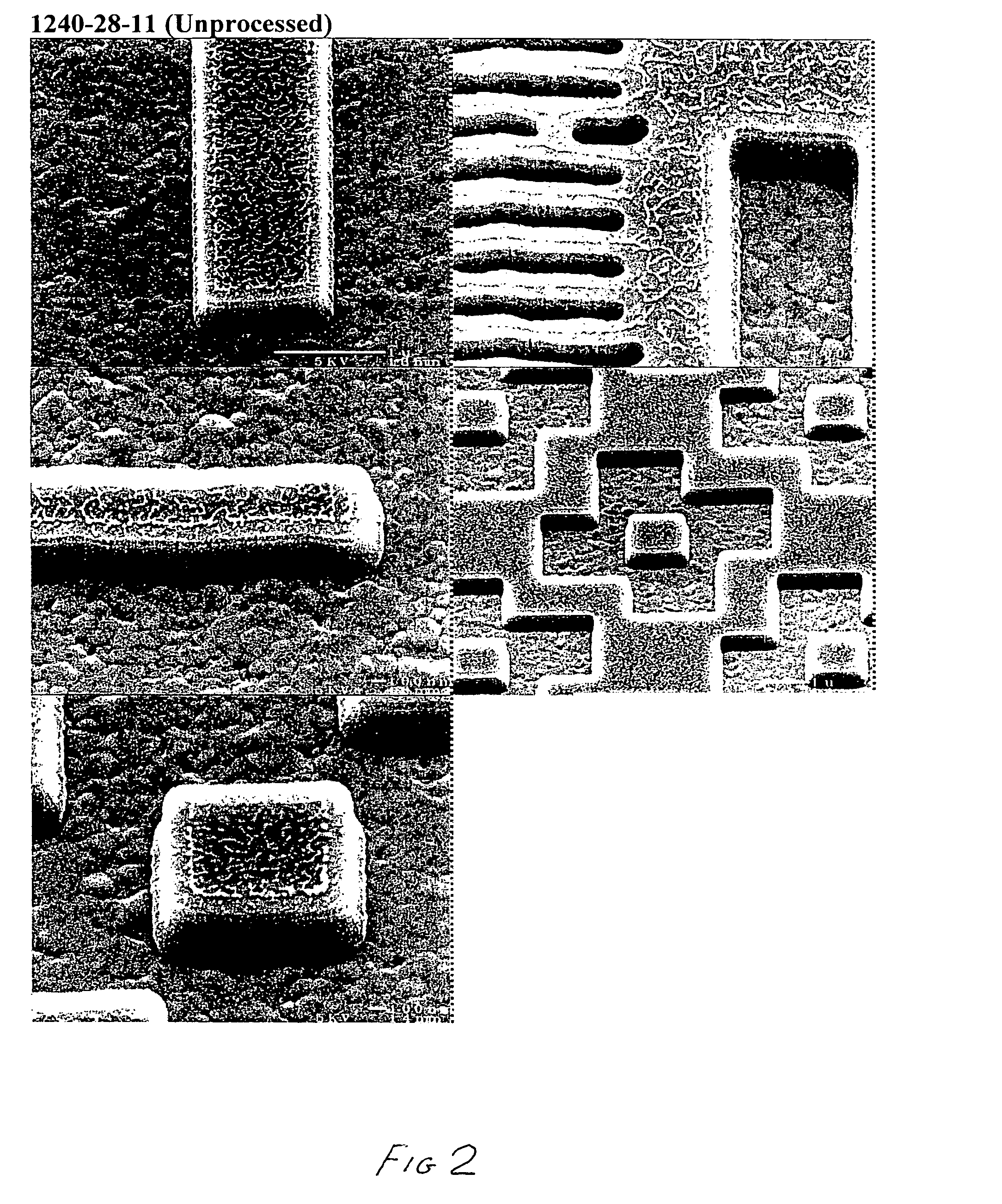
[0040] Cleaning copper-containing substrates following CMP processing are generally referred to as “post-Cu CMP” or “post-CMP copper clean”. A “copper-containing microelectronic substrate” is understood herein to refer to a substrate surface manufactured for use in microelectronic, integrated circuit, or computer chip applications, wherein the substrate contains copper-containing components. Copper-containing components may include, for example, metallic interconnects that are predominately copper or a copper alloy. It is understood that the microelectronic surface may also be composed of semiconductor materials, such as TiN, Ta, TiW (as copper diffusion barrier metals), and silica. Generally, a copper-containing microelectronic substrate contains about 1-20% Cu, including the copper interconnects.

[0041] The cleaning solution of the invention may find application for any cleaning operation during the fabrication of microelectronic substrates, such as semiconductor wafers. Most nota...


PUM

PropertyMeasurementUnit
temperatureaaaaaaaaaa
temperaturesaaaaaaaaaa
sizeaaaaaaaaaa

Abstract

A cleaning solution is provided for cleaning copper-containing microelectronic substrates, particularly for post etch, post-CMP or Via formation cleaning. The cleaning solution comprises a quaternary ammonium hydroxide, an organic amine, a corrosion inhibitor, and water. A preferred cleaning solution comprises tetramethylammonium hydroxide, monoethanolamine, gallic acid, and water. The pH of cleaning solution is greater than 10.

Description

FIELD OF THE INVENTION [0001] The present invention relates to post etch and post chemical-mechanical polishing (post-CMP) cleaning operations, and more specifically to post etch and post-CMP cleaning solutions for copper-containing microelectronic substrates. BACKGROUND OF THE INVENTION [0002] The present day fabrication of semiconductor devices is a complex, multi-step process. The CMP process and post etch processes are now well established enabling technology used by most advanced semiconductor operations for manufacturing of semi-conductor devices with design geometries less than 0.35 micron. [0003] The CMP processes involve holding and rotating a thin, flat substrate of the semiconductor material against a wetted polishing surface under controlled chemical, pressure and temperature conditions. A chemical slurry containing a polishing agent, such as alumina or silica, is used as the abrasive material. In addition, the chemical slurry contains selected chemicals which etch vario...

Claims


Application Information

Patent Timeline
Patent Type & Authority Applications(United States)
IPC IPC(8): C11D7/32
CPCC11D1/04C11D1/146C11D1/72C11D3/43C11D3/48C11D7/263C11D7/265C11D7/34C11D7/5031
Inventor PETERS, DARRYL W.OLDAK, EWA B.WALKER, ELIZABETH L.BARNES, JEFFREY A.NAGHSHINEH, SHAHRIAR
Owner ADVANCED TECH MATERIALS INC
Why Eureka
Try Eureka