Method and system for finding an equivalent circuit representation for one or more elements in an integrated circuit

a technology of integrated circuits and equivalent circuits, applied in the field of integrated circuit design, can solve the problems of unavoidable manufacturing process variations, integrated circuit element shapes printed on wafers often fail to match the element shapes drawn by the designer with an acceptable level of accuracy, and irregular lithography simulation shapes, etc., to reduce the processing time of analysis

Inactive Publication Date: 2006-07-06
RPX CORP
View PDF4 Cites 62 Cited by
  • Summary
  • Abstract
  • Description
  • Claims
  • Application Information

AI Technical Summary

Benefits of technology

[0011] Another object of the invention is to reduce the processing time of th

Problems solved by technology

However, not even leading-edge photomask making and other related technologies can compensate for unavoidable manufacturing process variations.
As a result of such process variations, the integrated circuit element shapes printed on the wafer often fail to match the element shapes drawn by the designer with an acceptable level of accuracy.
The lithography-simulated shapes can be irregular, and known circuit analysis tools are unable to handle the complexity of these shapes efficiently.
Since the underlying computer data structures and algorithms are dramatically simplified and have faster runtimes when straight-line edges and/or axis-parallel edges are assumed, existing circuit analysis tools have been limited to these types of primitive shapes.
These circuit analysis tools cannot inherently analyze complex lithography-simulated shapes.
Further, the runtime of parasitic ex

Method used


Image

  • Method and system for finding an equivalent circuit representation for one or more elements in an integrated circuit
  • Method and system for finding an equivalent circuit representation for one or more elements in an integrated circuit
  • Method and system for finding an equivalent circuit representation for one or more elements in an integrated circuit

Examples


Embodiment Construction

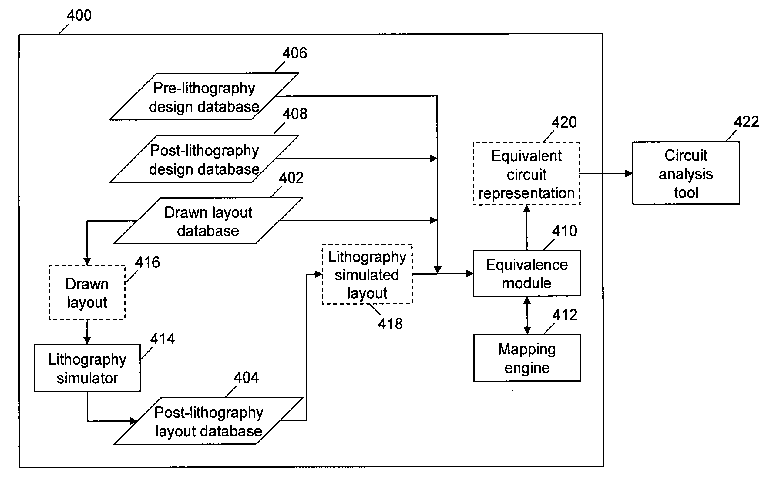
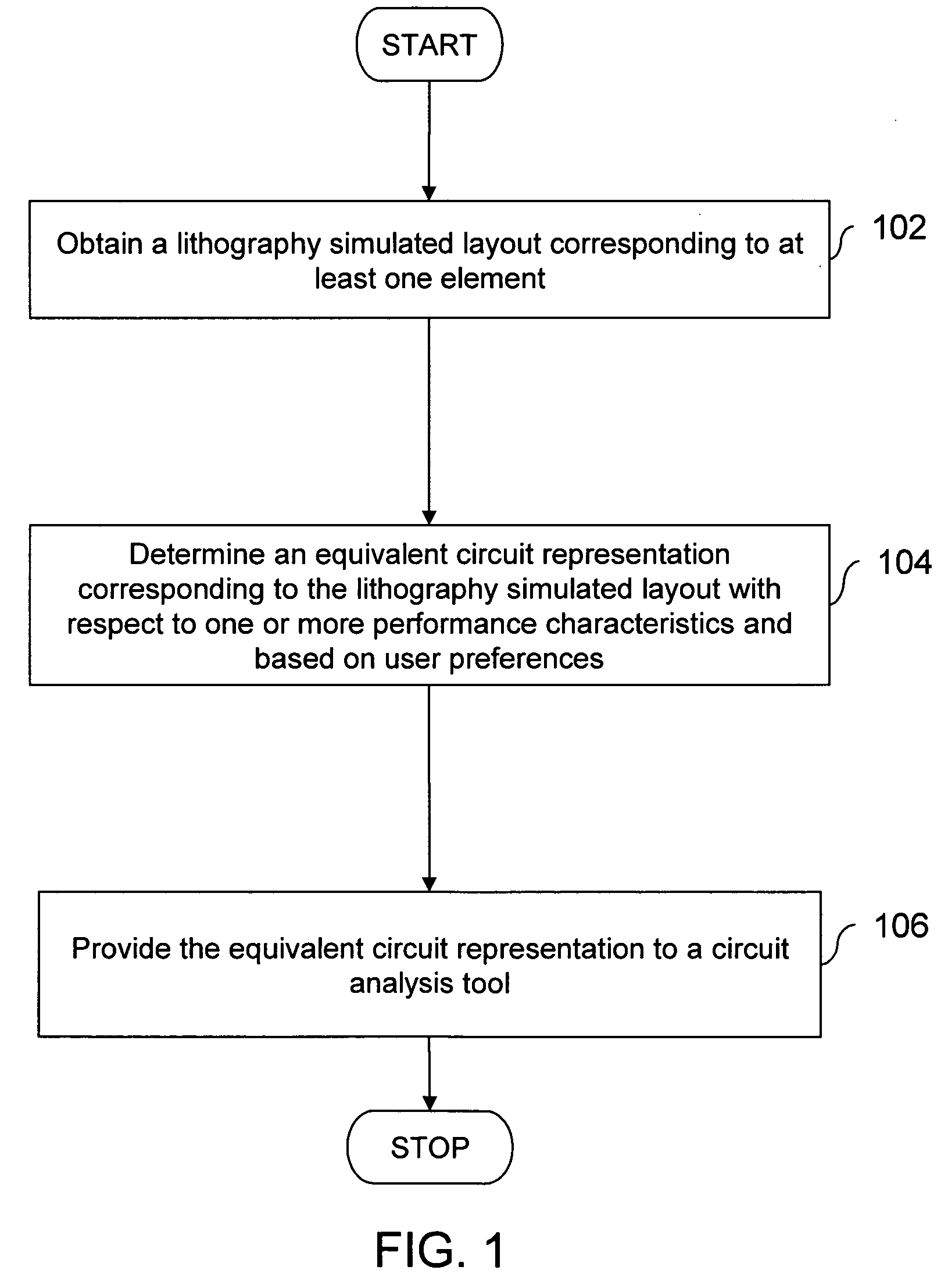
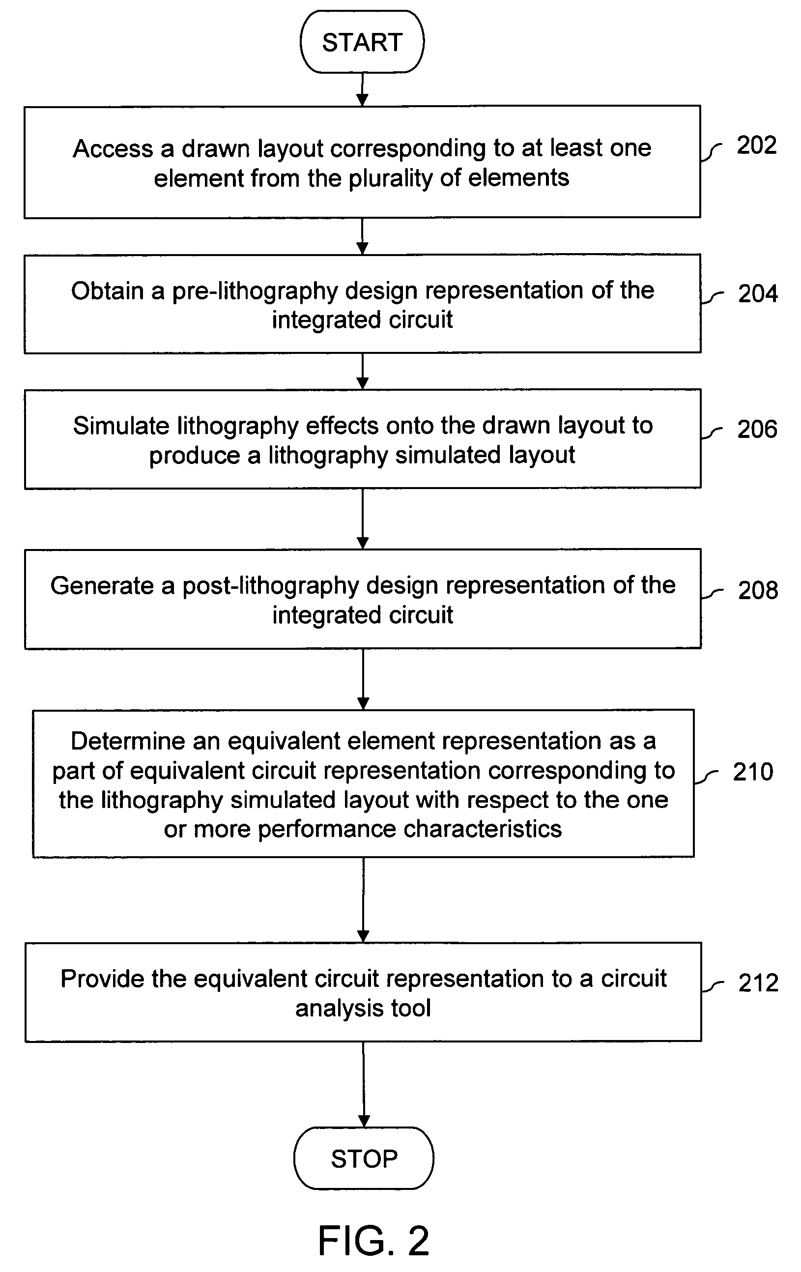
[0026] In a conventional approach for designing an integrated circuit (IC), the IC is represented by a drawn layout. The drawn layout is a description of the ideal, physical layout of the IC or circuit elements on the IC. GDSII is a common format for the drawn layout. In an ideal situation, the lithography-simulated layout of the circuit elements would match their drawn layout. Examples of circuit elements include a poly gate, a poly interconnect, a contact, a metal interconnect via or any other feature present in the layout of the integrated circuit. The circuit elements are hereinafter referred to as elements. The drawn layout may be referred to as a pre-lithography layout, since it is a representation of the IC, without accounting for lithography effects on the IC. The lithography-simulated layout, on the other hand, is a simulation of lithography effects on the drawn layout before the actual lithography, i.e., manufacturing or printing on the wafer, is performed on the elements....


PUM


Abstract

The present invention provides a method and a system for designing an integrated circuit comprising a plurality of elements. The method includes obtaining a lithography-simulated layout corresponding to at least one element. The lithography-simulated layout accounts for lithography effects on the element. The method further includes determination of an equivalent circuit representation that is compatible to a circuit analysis tool, corresponding to the lithography-simulated layout with respect to one or more performance characteristics and based on user preferences. The method also provides equivalent circuit representation to the circuit analysis tool that analyzes one or more performance characteristics of the elements.

Description

CLAIM OF PRIORITY [0001] This application claims priority of U.S. provisional application Ser. No. 60 / 640,917 filed Dec. 31, 2004, entitled System and Method for Calculation and Use of Equivalent Shapes in the Design of Integrated CircuitsBACKGROUND OF THE INVENTION [0002] 1. Field of the Invention [0003] This invention relates generally to the design of integrated circuits (ICs), and more particularly, to the performance analysis of ICs. [0004] 2. Description of the Related Art [0005] In the manufacture of modern integrated circuits, the size of circuit elements has been reduced to the nanometer scale. Each new technological advancement entails tighter manufacturing process control requirements. For example, in the optical lithography process, circuit element sizes are significantly smaller than the wavelength of light used in optical lithography, resulting in a “sub-wavelength lithography” regime. This requires advanced photomasks that embody one or more reticle enhancement techni...

Claims


Application Information

Patent Timeline
IPC IPC(8): G06F17/50G06F9/45
CPCG03F7/70433G03F7/705G06F17/5036G06F17/5081G06F30/367G06F30/398
Inventor GUPTA, PUNEET
Owner RPX CORP
Why Eureka
Try Eureka