MOSFET device with localized stressor

a stressor and mosfet technology, applied in the field of metal oxidesemiconductor field-effect transistors, can solve the problems of junction leakage, difficult processing, and difficult control of the level of germanium in the epitaxially grown semiconductor alloy layer, and achieve the effect of improving the operating characteristics of the semiconductor device and a method

Inactive Publication Date: 2006-07-13
TAIWAN SEMICON MFG CO LTD
View PDF14 Cites 73 Cited by
  • Summary
  • Abstract
  • Description
  • Claims
  • Application Information

AI Technical Summary

Benefits of technology

[0007] These and other problems are generally reduced, solved or circumvented, and technical advantages are generally achieved, by embodiments of the presen

Problems solved by technology

This approach, however, can be difficult to process in addition to presenting junction leakage concerns as a result of the blanket semiconductor alloy layer.
The level of germanium in the epitaxially grown semiconductor alloy layer can be difficult to control.
In addition, the presence of a blanket semiconductor alloy layer allows an unwanted interface between the source

Method used


Image

  • MOSFET device with localized stressor
  • MOSFET device with localized stressor
  • MOSFET device with localized stressor

Examples


Embodiment Construction

[0016] The making and using of the presently preferred embodiments are discussed in detail below. It should be appreciated, however, that the present invention provides many applicable inventive concepts that can be embodied in a wide variety of specific contexts. The specific embodiments discussed are merely illustrative of specific ways to make and use the invention, and do not limit the scope of the invention.

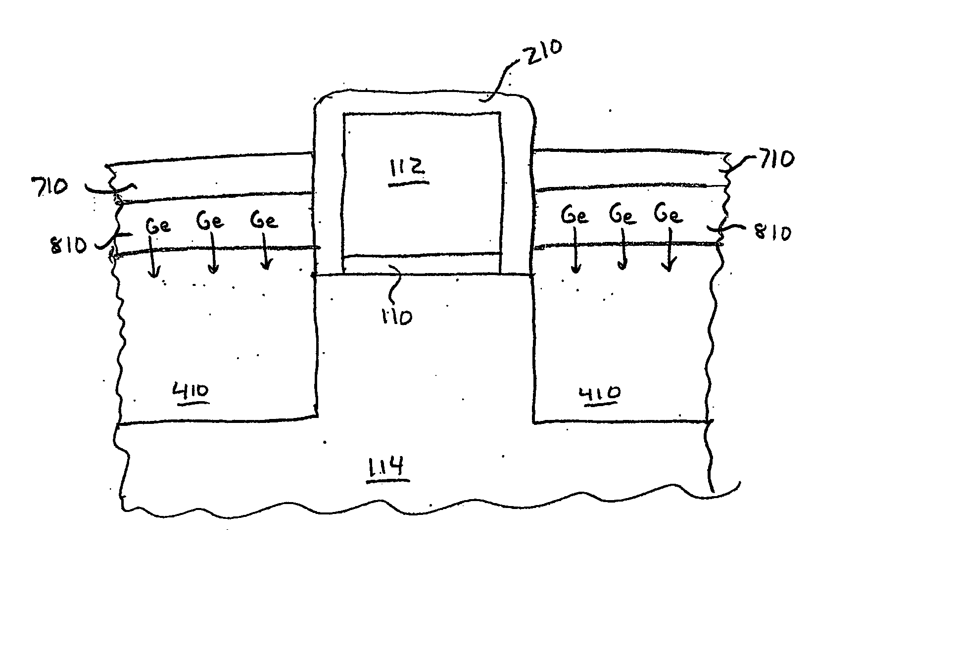
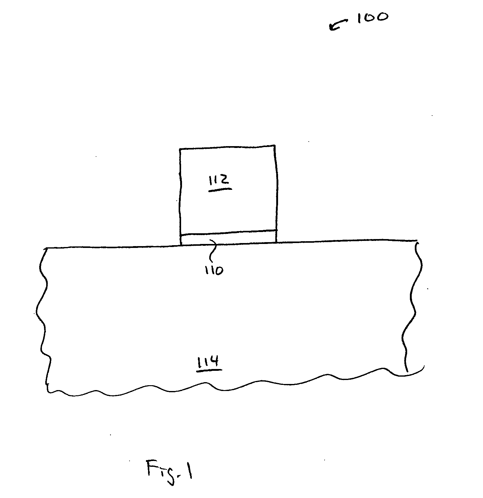
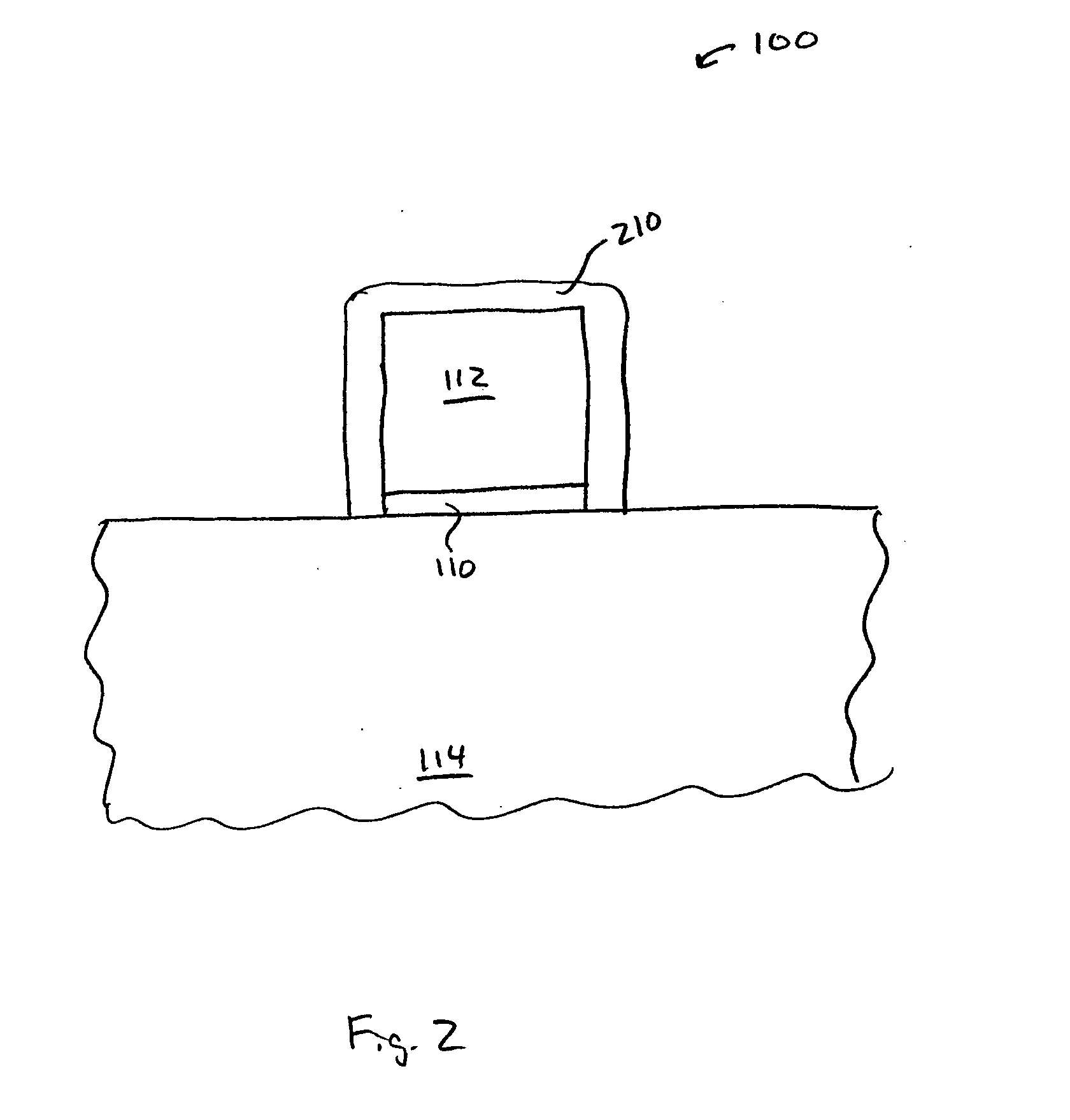
[0017]FIGS. 1-6 illustrate a method embodiment for fabricating a semiconductor device having a strained channel region in accordance with an embodiment of the present invention. Embodiments of the present invention illustrated herein may be used in a variety of circuits. Referring first to FIG. 1, a wafer 100 having a gate insulator layer 110 and a gate electrode 112 formed on a substrate 114 is shown in accordance with an embodiment of the present invention. The substrate 114 may comprise bulk silicon, doped or undoped, or an active layer of a semiconductor-on-insulator (S...


PUM


Abstract

MOSFETs having localized stressors are provided. The MOSFET has a stress-inducing layer formed in the source/drain regions, wherein the stress-inducing layer comprises a first semiconductor material and a second semiconductor material. A treatment is performed on the stress-inducing layer such that a reaction is caused with the first semiconductor material and the second semiconductor material is forced lower into the stress-inducing layer. The stress-inducing layer may be either a recessed region or non-recessed region. A first method involves forming a stress-inducing layer, such as SiGe, in the source/drain regions and performing a nitridation or oxidation process. A nitride or oxide film is formed in the top portion of the stress-inducing layer, forcing the Ge lower into the stress-inducing layer. Another method embodiment involves forming a reaction layer over the stress-inducing layer and performing a treatment process to cause the reaction layer to react with the stress-inducing layer.

Description

TECHNICAL FIELD [0001] The present invention relates generally to semiconductor devices, and more particularly, to metal-oxide-semiconductor field-effect transistors and methods of manufacture. BACKGROUND [0002] Size reduction of metal-oxide-semiconductor field-effect transistors (MOSFET), including reduction of the gate length and gate oxide thickness, has enabled the continued improvement in speed, performance, density, and cost per unit function of integrated circuits over the past few decades. To further enhance transistor performance, MOSFET devices have been fabricated using strained channel regions located in portions of a semiconductor substrate. Strained channel regions allow enhanced carrier mobility to be realized, thereby resulting in increased performance when used for n-channel (NMOSFET) or for p-channel (PMOSFET) devices. Generally, it is desirable to induce a tensile strain in the n-channel of an NMOSFET transistor in the source-to-drain direction to increase electro...

Claims


Application Information

Patent Timeline
IPC IPC(8): H01L31/109H01L21/8234H01L21/477
CPCH01L21/26506H01L21/28518H01L21/823807H01L29/165H01L29/517H01L29/518H01L29/66636H01L29/7834H01L29/7848H01L21/28525H01L29/45H01L29/66628H04N19/115H04N19/126H04N19/40H04N19/48
Inventor CHEN, CHIEN-HAOTSAI, PANG-YENCHANG, CHIE-CHIENLEE, TZE-LIANGCHEN, SHIH-CHANG
Owner TAIWAN SEMICON MFG CO LTD
Why Eureka
Try Eureka