Hot carrier degradation reduction using ion implantation of silicon nitride layer

a technology of silicon nitride and hot carrier, which is applied in the direction of semiconductor devices, electrical apparatus, transistors, etc., can solve the problems of device degradation, enhanced substrate current, and trapped gate oxide, and achieve the effect of reducing hot carrier degradation

Inactive Publication Date: 2006-07-13
IBM CORP +1
View PDF3 Cites 6 Cited by
  • Summary
  • Abstract
  • Description
  • Claims
  • Application Information

AI Technical Summary

Benefits of technology

[0011] A third aspect of the invention is directed to a method of reducing hot carrier degradation in a transistor device, the method comprising the steps of: depositing a silicon nitride layer over a plurality of transistor devices; forming a mask revealing a particular transistor device; ion implanting a species into the silicon nitride layer t...

Problems solved by technology

First, if the hot carriers attain enough energy, they can surmount the silicon-silicon dioxide (Si—SiO2) barrier of the substrate and gate oxide and become trapped in the gate oxide.
Trapped charges cause device degradation and enhanced substrate current (ISUB), and affect the device's threshold voltage.
Second, hot carriers can lead to avalanche breakdown when they form enough electron-hole pairs that current ceases flowing to the drain.
Accordingly, hot carrier degra...

Method used


Image

  • Hot carrier degradation reduction using ion implantation of silicon nitride layer
  • Hot carrier degradation reduction using ion implantation of silicon nitride layer
  • Hot carrier degradation reduction using ion implantation of silicon nitride layer

Examples


Embodiment Construction

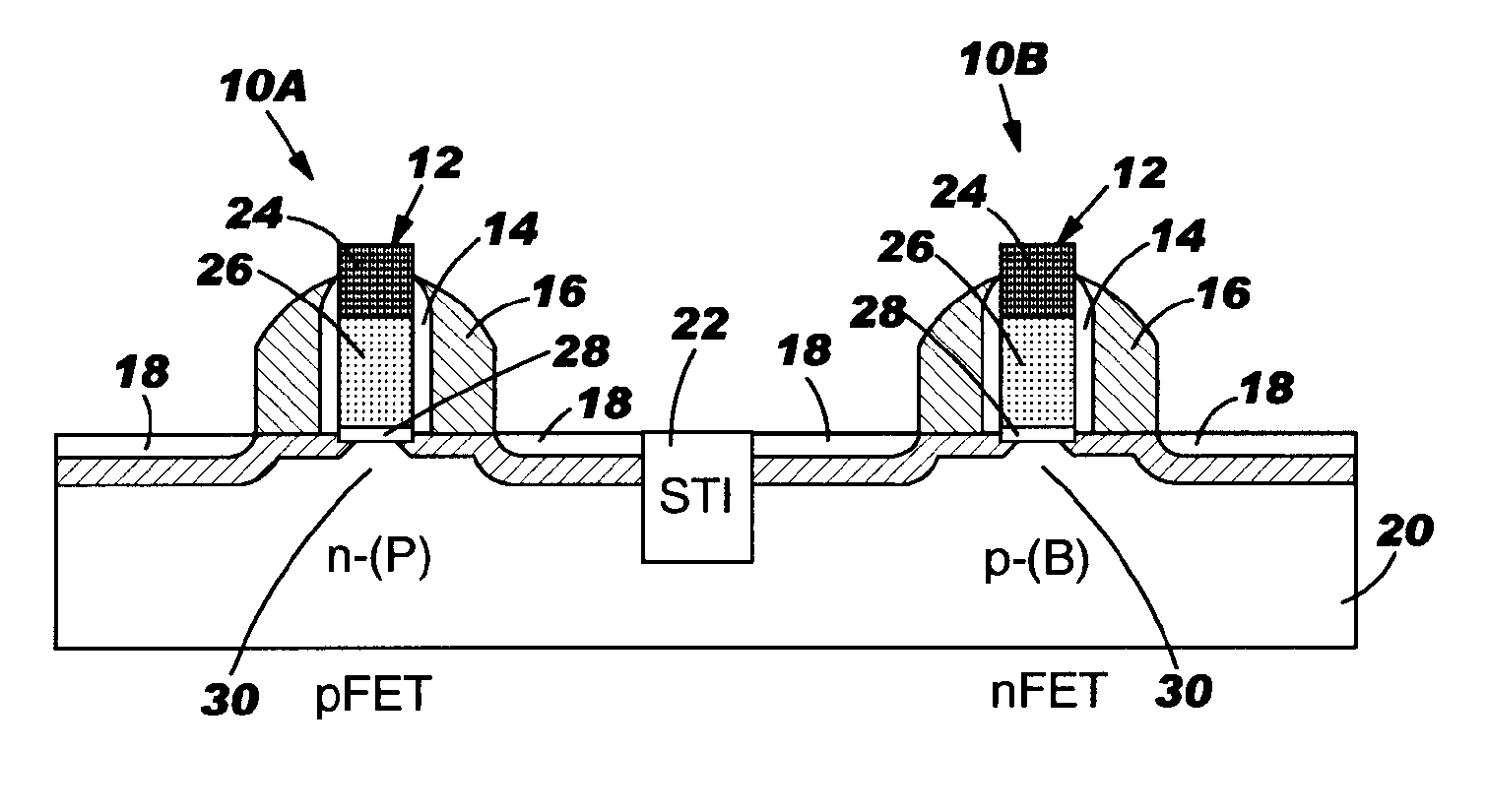
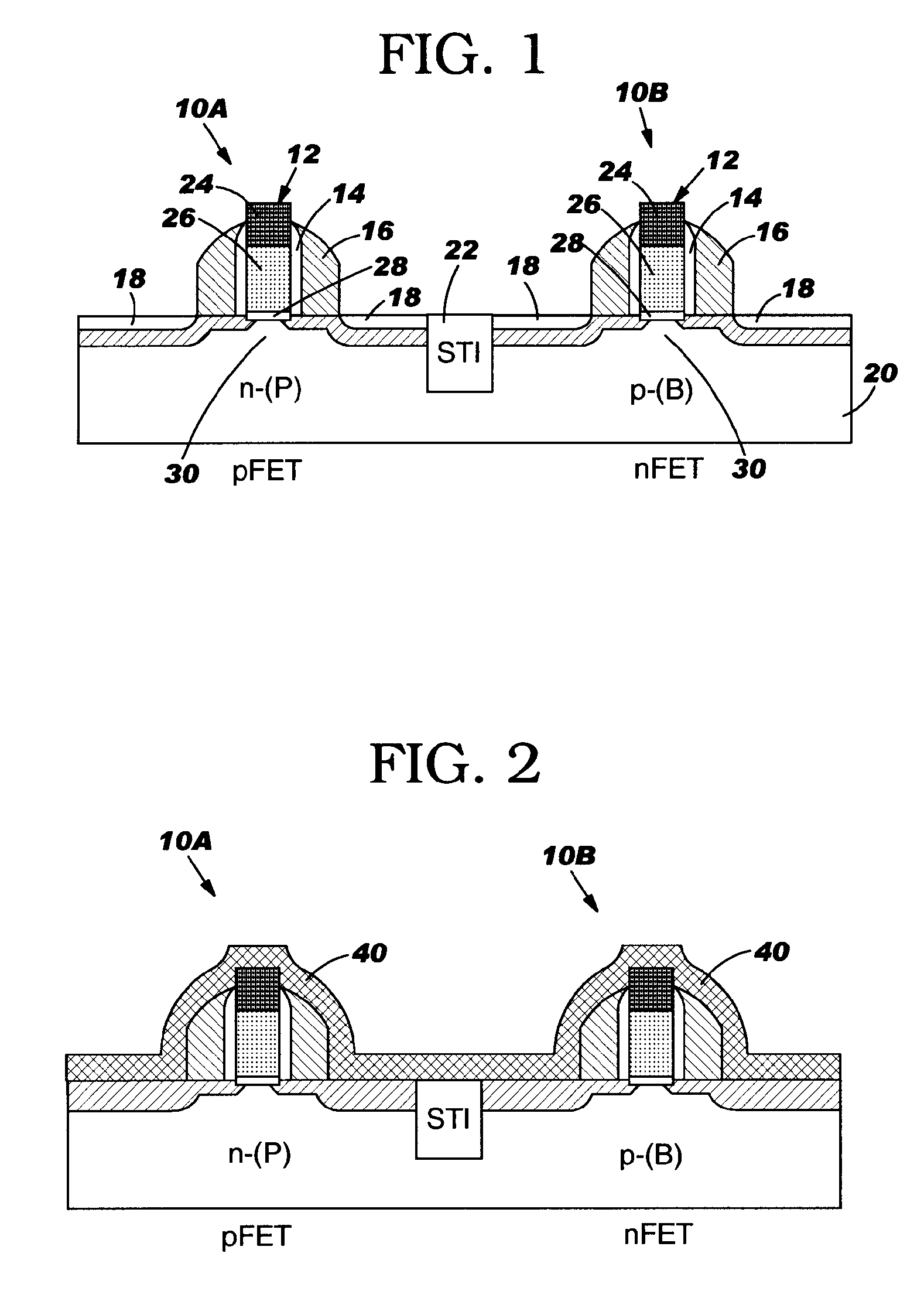
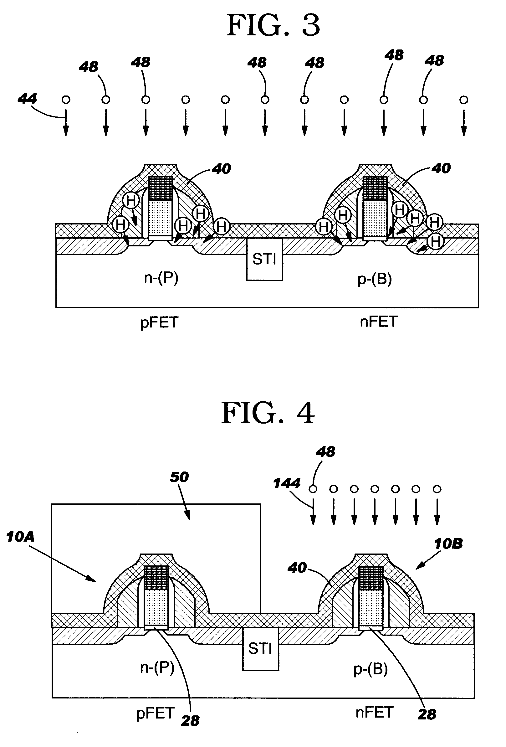
[0016] With reference to the accompanying drawings, FIGS. 1-5 show a method of reducing hot carrier degradation in a transistor device according to the invention. As shown in FIG. 1, an initial structure includes at least one transistor device 10A, 10B including, for example, a gate 12, surrounded by an inner 14 and outer spacer 16, and a source / drain region 18 positioned within a substrate 20. Substrate 20 also includes a shallow trench isolation (STI) 22 to separate different transistor devices 10. Gate 12 includes a silicide cap 24, a polysilicon body 26 and a gate silicon dioxide region 28 (hereinafter “gate oxide”). Each gate 12 is positioned over a channel region 30. As illustrated, transistor device 10A is a p-type field effect transistor (pFET) and transistor device 10B is an n-type field effect transistor (nFET), however, transistor devices 10A, 10B can be any type transistor device.

[0017]FIG. 2 illustrates a first step of one embodiment of a method of reducing hot carrier...


PUM


Abstract

A method of reducing hot carrier degradation and a semiconductor structure so formed are disclosed. One embodiment of the method includes depositing a silicon nitride layer over a transistor device, ion implanting a species into the silicon nitride layer to drive hydrogen from the silicon nitride layer, and annealing to diffuse the hydrogen into a channel region of the transistor device. The species may be chosen from, for example: germanium (Ge), arsenic (As), xenon (Xe), nitrogen (N), oxygen (O), carbon (C), boron (B), indium (In), argon (Ar), helium (He), and deuterium (De). The ion implantation modulates atoms in the silicon nitride layer such as hydrogen, nitrogen and hydrogen-nitrogen bonds such that hydrogen can be controllably diffused into the channel region.

Description

BACKGROUND OF THE INVENTION [0001] 1. Technical Field [0002] The present invention relates generally to semiconductor fabrication, and more particularly, to methods and a semiconductor structure formed thereby for reducing hot carrier degradation using ion implantation of a silicon nitride layer. [0003] 2. Related Art [0004] During operation of a transistor device, an electric field is formed between a source and drain region, i.e., in a channel, by the application of a voltage to a gate such that current can flow between the source and drain. Conventional, ultra-large semiconductor integrated circuits (ULSI) feature extremely short channel lengths and high electric fields. In these high electric fields, carriers are accelerated to high velocities, reaching a maximum kinetic energy (hot) near the device drain. If the carrier energy is high enough, impact ionization can occur, creating electron-hole pairs, also referred to as hot carriers. Holes are positive charge carriers that mate...

Claims


Application Information

Patent Timeline
IPC IPC(8): H01L29/94
CPCH01L21/26506H01L21/823807H01L29/1033H01L29/4933H01L29/6659H01L29/7833H01L29/7842H01L29/7843H01L21/26513
Inventor YANG, HAININGCHEN, XIANGDONGLEE, YONG MENGLIN, WENHE
Owner IBM CORP
Why Eureka
Try Eureka