Method of forming a nanogap and method of manufacturing a nano field effect transitor for molecular device and bio-sensor, and molecular device and bio-sensor manufactured using the same

a technology of nano-gaps and nano-fields, which is applied in the direction of photomechanical devices, originals for photomechanical treatment, instruments, etc., can solve the problems of limiting the scaledown of the device, the technical limit of the method of forming a gap of molecular length using the conventional lithography process, and the limitation of the manufacturing method

Inactive Publication Date: 2006-07-13
KOREA ADVANCED INST OF SCI & TECH
View PDF11 Cites 41 Cited by
  • Summary
  • Abstract
  • Description
  • Claims
  • Application Information

AI Technical Summary

Benefits of technology

[0029] A method of manufacturing a nano field effect transistor for a molecular device using the vertical nanogap, comprising steps of a) forming sequentially an insulating layer, a first silicon nitride (Si3N4) layer and a first metal layer on a silicon substrate; b) forming sequentially a first dielectric layer, a second metal layer, a second silicon nitride layer and a hard mask on the structure formed on the silicon substrate; c) etching partially the second silicon nitride layer, the second metal layer, the first dielectric layer, the first metal layer and the first silicon nitride layer using the hard mask as an etching mask; d) forming a second dielectric layer, which can be formed and etched anisotropically, on the entire structure; e) etching the second dielectric layer through an etch-back process to form gate oxide layers; f) depositing a gate material on the entire structure; g) etching the gate material deposited in step (f) using a photoresist pattern as the mask to form a gate; h) etching the first dielectric layer formed in step (b) to form the vertical nanogap; and i) forming a molecular layer in the vertical nanogap formed in step (h), the molecular layer having a length which is same as the width of the nanogap.

Problems solved by technology

Due to the technological limitations (light source wavelengths, light dispersions, lens numerical aperture (N / A), and absence of photoresist) of the lithography method used in a semiconductor manufacturing process, scaledown of the device now gets to the limit.
As noted above, however, a method of forming a gap of molecular length using the conventional lithography process has reached a technical limit.
However, forming the gap of a size smaller than several nanometers by means of the lithography process used for the conventional silicon processing has the technical limitations such as the wavelength of the light source to be used, the dispersion phenomenon of light and the like.
Moreover, since the formation of a nanogap using the lithography method requires a complicated process and its reproducibility become lower as the desired gap size becomes smaller, the formation of the several nanometers sized gap required for the high performance bio-sensor is difficult to form.

Method used


Image

  • Method of forming a nanogap and method of manufacturing a nano field effect transitor for molecular device and bio-sensor, and molecular device and bio-sensor manufactured using the same
  • Method of forming a nanogap and method of manufacturing a nano field effect transitor for molecular device and bio-sensor, and molecular device and bio-sensor manufactured using the same
  • Method of forming a nanogap and method of manufacturing a nano field effect transitor for molecular device and bio-sensor, and molecular device and bio-sensor manufactured using the same

Examples


Embodiment Construction

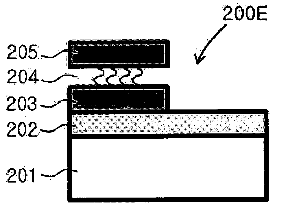
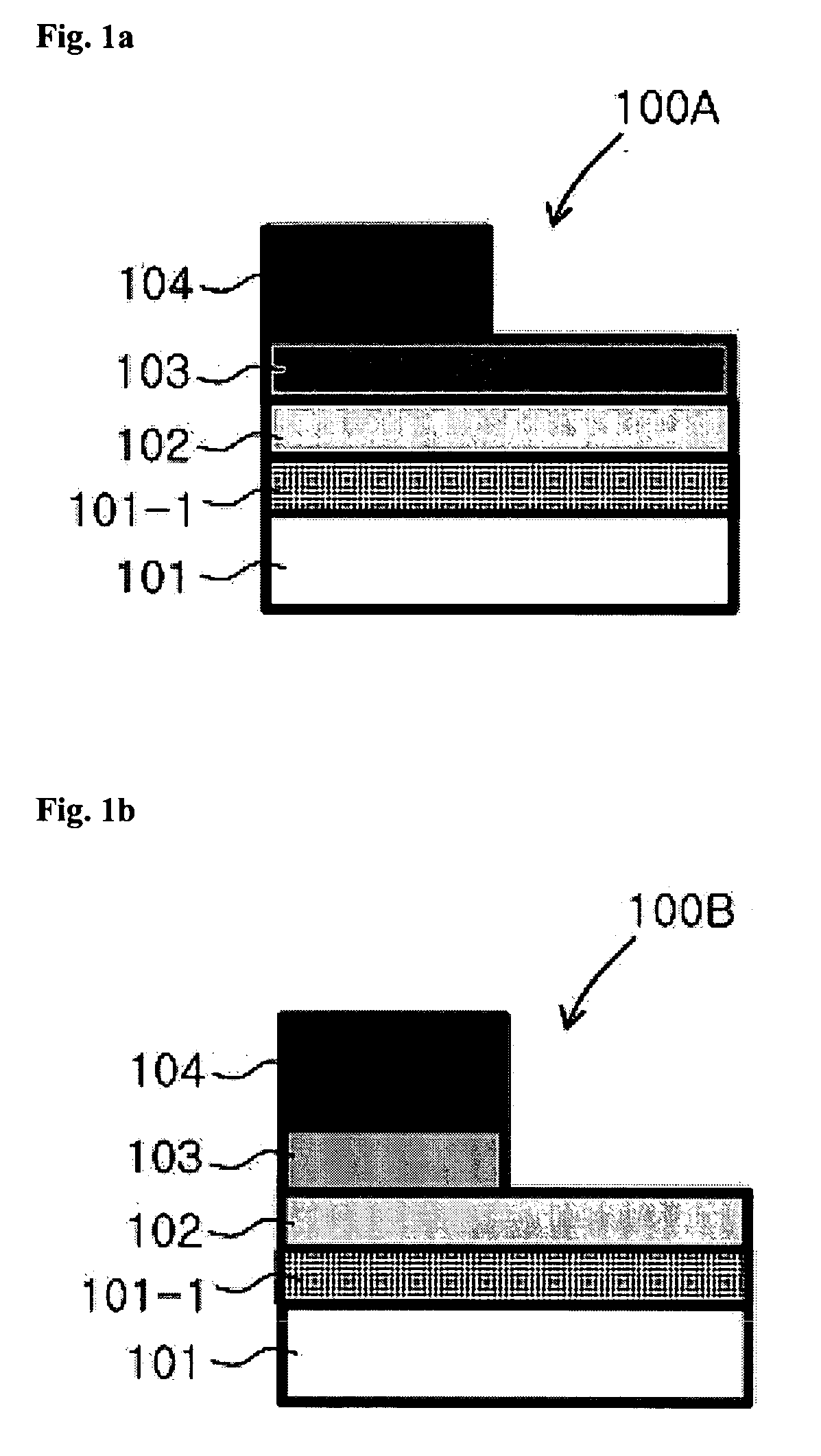
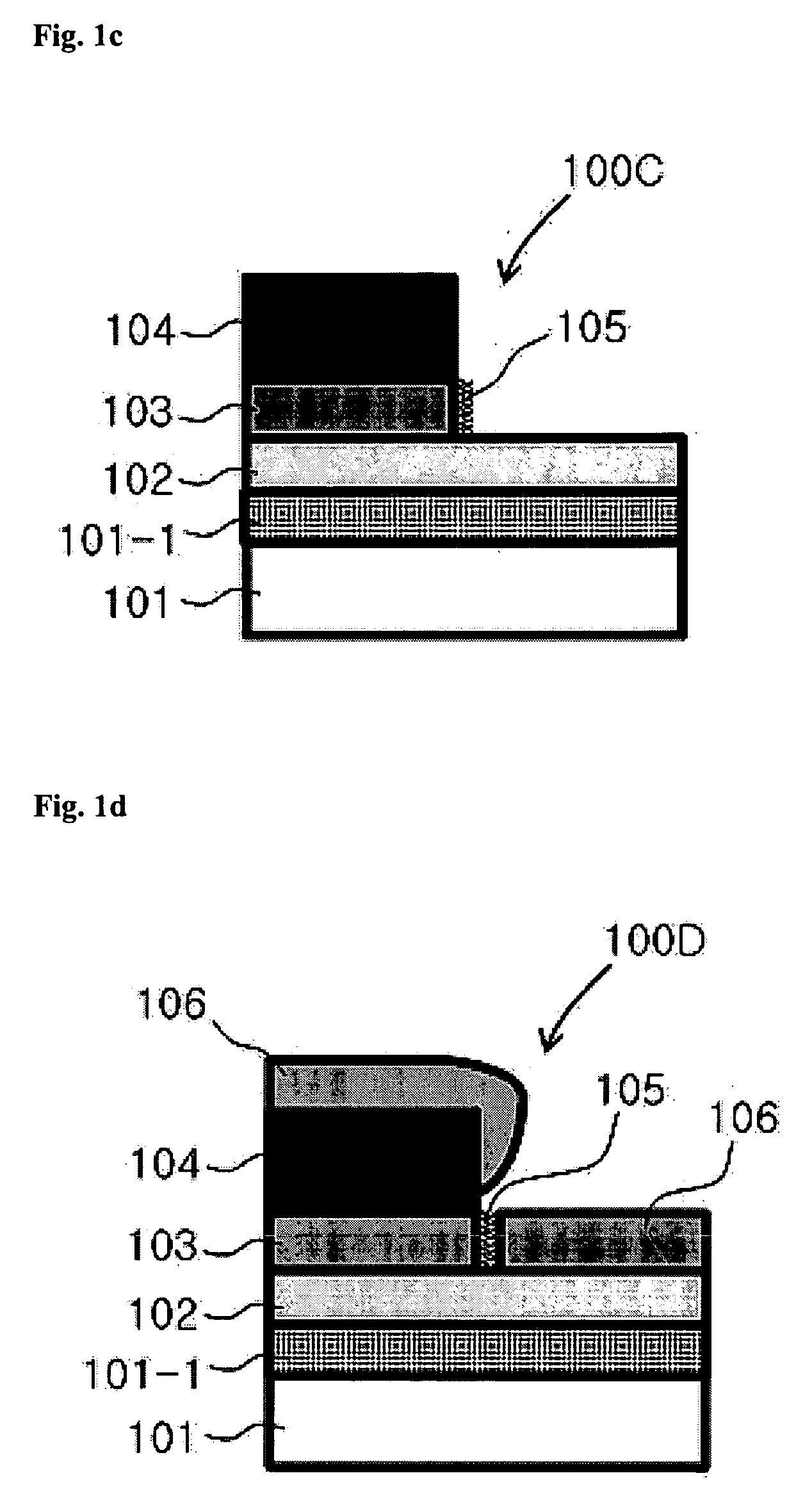
[0039] Hereinafter, a method of forming a nanogap for a molecular device or a bio-sensor and a method of manufacturing a nano field effect transistor for a molecular device or a bio-sensor according to the preferred embodiment of the present invention will be described in detail with reference to the accompanying drawings.

[0040]FIG. 1A to FIG. 1F are sectional views showing sequentially a method of forming a planar nanogap for a bio-sensor according to one embodiment of the present invention.

[0041] As shown in the drawings, a first aurum (Au) layer (metal layer) is formed on a silicon substrate, and a second Au layer spaced apart from the first Au layer is formed by using a self-assembled monolayer (hereinafter, referred to as “SAM”), so a planar nanogap corresponding to a length of the SAM is formed.

[0042] A process for forming the nanogap is described in detail as follows.

[0043] First, a back-gate thin layer 101-1 to be formed by a doping process, an insulating layer 102, a fi...


PUM

PropertyMeasurementUnit
lengthaaaaaaaaaa
widthaaaaaaaaaa
molecular sizeaaaaaaaaaa

Abstract

The present invention relates to a method of forming a nanogap, a method of manufacturing a nano field effect transistor for a molecular device or a bio-sensor, and a fabrication thereof, and more particularly, to a method of forming a high reproductive nanogap using a thin layer with a molecular size or a size which is similar to that of a molecule and a nano field effect transistor manufactured by the method of forming the nanogap. The method of forming a nanogap according to the present invention comprises steps of (a) forming sequentially an insulating layer, a first metal layer and a hard mask on a silicon substrate; (b) etching partially the first metal layer using the mask as an etching mask; (c) forming a self-assembled monolayer (SAM) on a side surface of the first metal layer to form a nanogap on the silicon substrate; (d) depositing metal on the entire structure including the mask to form a second metal layer; (e) removing the metal deposited on the hard mask using a lift-off process by etching the mask formed in step (a) and (f) etching the SAM formed in step (c) to form the nanogap.

Description

[0001] This Nonprovisional application claims priority under 35 U.S.C. § 119(a) on Patent Application No. 10-2005-0002294 filed in Korea on Jan. 10, 2005, the entire contents of which are hereby incorporated by reference. BACKGROUND OF THE INVENTION [0002] 1. Field of the Invention [0003] The present invention relates to a method of forming a nanogap, a manufacturing method and a structure of a nano field effect transistor (nanoFET) for a molecular device or a bio-sensor, and more particularly, to a method of forming a highly reproducable nanogap using a film as thin as a molecular size or as a size similar to the molecular size, and to a nano field effect transistor manufactured by the method of forming the nanogap. [0004] 2. Description of the Background Art [0005] A metal nanogap in which metal plates are located both sides of a nanometer sized gap is valuable in manufacturing a molecular device and a bio-sensor. [0006] With continuous technological developments, a high integrati...

Claims


Application Information

Patent Timeline
Patent Type & Authority Applications(United States)
IPC IPC(8): H01L21/00G03C5/00
CPCB82Y10/00B82Y15/00B82Y30/00G01N33/54373G01N33/552G01N33/553G01N2610/00F16F1/38F16F15/08
Inventor CHOI, YANG-KYUKIM, JU-HYUN
Owner KOREA ADVANCED INST OF SCI & TECH
Why Eureka
Try Eureka