Semiconductor device and manufacturing method thereof

a manufacturing method and semiconductor technology, applied in the direction of semiconductor devices, electrical devices, transistors, etc., can solve the problems of crystallinity defects, achieve excellent crystallinity, ensure high-performance semiconductor integrated circuits, and use excellent various characteristics of semiconductor devices

Inactive Publication Date: 2006-07-13
HITACHI LTD
View PDF6 Cites 13 Cited by
  • Summary
  • Abstract
  • Description
  • Claims
  • Application Information

AI Technical Summary

Benefits of technology

[0031] According to a manufacturing method of a semiconductor device of the present invention, a semiconductor layered product having excellent crystallinity can be achieved, thereby, excellent various characteristics of the semiconductor device using this can be ensured. Or, high performance of the semiconductor integrated circuit can be ensured.

Problems solved by technology

In a manufacturing method of a semiconductor single-crystal multilayer disclosed in prior arts, there are problems like the ones that follow because hydrogen is continuously supplied until growth of the n-type single-crystal SiGe layer is started in the second reactor after finishing the p-type single-crystal SiGe layer in the first reactor.
Therefore, in prior arts in which hydrogen is supplied during transfer, oxygen atoms are adsorbed at the surface when the substrate temperature is low, so that there is a problem that crystal defects are created by oxygen being taken in at the interface of the semiconductor single-crystal multilayer film.

Method used


Image

  • Semiconductor device and manufacturing method thereof
  • Semiconductor device and manufacturing method thereof
  • Semiconductor device and manufacturing method thereof

Examples


first embodiment

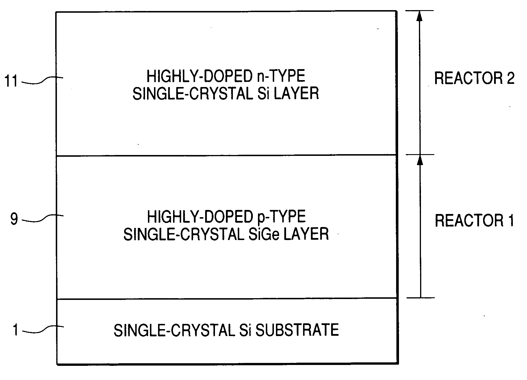
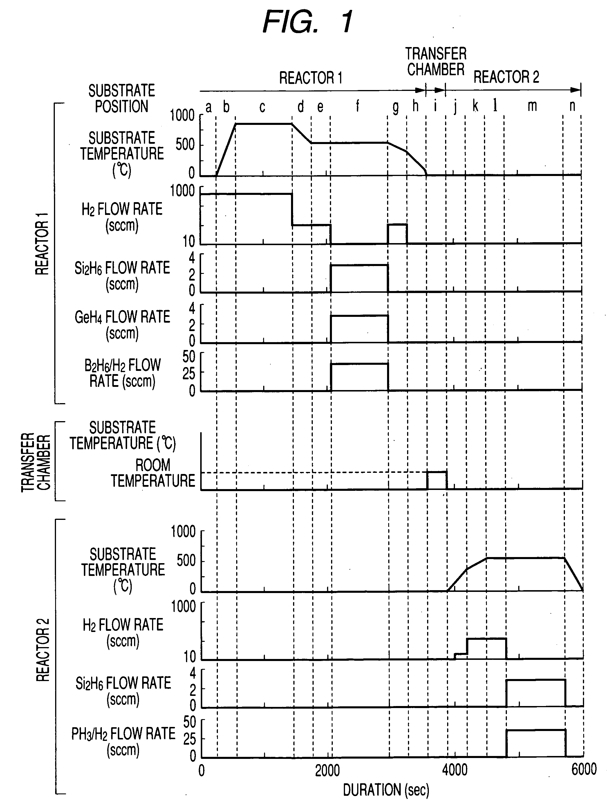
[0055]FIG. 1 is a drawing illustrating a sequence of the first embodiment of the present invention. This shows a sequence to form a multilayer film consisting of a highly-doped p-type single-crystal SiGe layer and a highly-doped n-type single-crystal Si layer on a single-crystal Si substrate. Processes from step g to step l correspond to the second process in the present invention. In step g, the first crystal growth (the first process in the present invention) is completed and the second process starts. Then, hydrogen is supplied until the substrate temperature drops to a predetermined temperature, for instance, in the vicinity of 200° C. (step g). When the substrate temperature drops to the predetermined temperature or lower, the supply of hydrogen is stopped (step h and step i). In step j, the substrate temperature is increased for the purpose of the second crystal growth in the second reactor. In this step j, when the substrate temperature increases to the predetermined temperat...

second embodiment

[0072]FIG. 4 is a drawing illustrating a sequence of the second embodiment of the present invention. FIG. 4 shows a sequence to form a multilayer film consisting of a highly-doped p-type single-crystal SiGe layer 9 and a highly-doped n-type single-crystal Si layer 11 on a single-crystal Si substrate 1. The following points are the differences between the first embodiment and this embodiment. In the first embodiment, a highly-doped n-type single-crystal Si layer was grown in the second reactor on the highly-doped p-type single-crystal SiGe layer 9 grown in the first reactor 100. However, in this embodiment, a highly-doped n-type single-crystal Si layer is also grown in the first reactor 100 in which the highly-doped p-type single-crystal SiGe layer 9 was grown.

[0073] Processes from step g to step l correspond to the second process in the present invention. In step g, the first crystal growth (the first process in the present invention) is completed and the second process starts. The...

third embodiment

[0078]FIG. 6 shows the third embodiment of the present invention. FIG. 6 is a longitudinal section structure of a SiGe HBT. A semiconductor substrate comprising a highly-doped n-type single-crystal Si layer 2 to be a so-called buried layer, an n-type single crystal Si layer 3 to be part of a collector, a first collector / base isolation insulator film 4, a highly-doped n-type single-crystal Si layer 5 to be a collector lead layer, and an isolation insulator film 6, is formed on a Si substrate 1. Then, a second collector / base isolation insulator film 7 is formed on the surface of the substrate except for the parts on which an intrinsic region of the HBT and a collector lead layer are formed. On the n-type single-crystal Si layer 3 exposing the surface, an n-type single-crystal SiGe layer 8 to be a collector, a highly-doped p-type single-crystal SiGe layer 9 to be a base, and a highly-doped n-type single-crystal Si layer 11 to be an emitter are grown in order epitaxially. Moreover, a hi...


PUM


Abstract

A manufacturing method of a semiconductor device in which the oxygen and carbon concentrations are reduced at the interface of each layer making up the semiconductor multilayer film. A first semiconductor layer is formed on a single-crystal substrate in a first reactor; the substrate is transferred from the first reactor to a second reactor through a transfer chamber; and a second semiconductor layer is formed on the first semiconductor layer in the second reactor. During substrate transfer, hydrogen is supplied when the number of hydrogen atoms bonding with the surface atoms of the first semiconductor layer is less than the number of surface atoms of the first semiconductor layer, and the supply of hydrogen is stopped when the number of hydrogen atoms bonding with the surface atoms of the first semiconductor layer is greater than the number of surface atoms of the first semiconductor layer.

Description

CLAIM OF PRIORITY [0001] The present application claims priority from Japanese application JP 2005-004744 filed on Jan. 12, 2005, the content of which is hereby incorporated by reference into this application. FIELD OF THE INVENTION [0002] The present invention relates to a semiconductor device and a manufacturing method thereof, and more particularly to a manufacturing method of a semiconductor multilayer film with implementation of substrate transport. BACKGROUND OF THE INVENTION [0003] Recently, with the rapid development of large-capacity data transmission systems and ultra-high-speed wireless communication systems, improvement in the performance and the reduction in cost of LSIs used in them have been required. Therefore, since it has excellent operational speed and uses existing Si processes, attention has been paid to SiGe HBT technology. [0004] In order to improve the HBT performance, achieving a step doping profile is necessary to increase the cutoff frequency. Moreover, in...

Claims


Application Information

Patent Timeline
Patent Type & Authority Applications(United States)
IPC IPC(8): H01L21/20
CPCH01L21/02381H01L21/0245H01L21/02532H01L21/02576H01L21/02579H01L21/0262H01L29/1054H01L29/66242H01L29/66431H01L29/78
Inventor SUZUMURA, ISAOODA, KATSUYA
Owner HITACHI LTD
Why Eureka
Try Eureka