Optoelectronic architecture having compound conducting substrate cross-reference to related application

a technology of compound conducting substrate and optoelectronic device, which is applied in the manufacture of final products, sustainable manufacturing/processing, light radiation electric generators, etc., can solve the problems of premature failure of solder joints, incompatibility of solder and silicon wafer materials, and individual optoelectronic devices producing only a relatively small voltag

Inactive Publication Date: 2006-07-20
AERIS CAPITAL SUSTAINABLE IP
View PDF99 Cites 196 Cited by
  • Summary
  • Abstract
  • Description
  • Claims
  • Application Information

AI Technical Summary

Problems solved by technology

Currently, there are a number of technical challenges to attaining this goal.
A further problem associated with existing solar fabrication techniques arises from the fact that individual optoelectronic devices produce only a relatively small voltage.
Unfortunately the solder and silicon wafer materials were not compatible.
The differing rates of thermal expansion between silicon and solder and the rigidity of the wafers caused premature failure of the solder joints with temperature cycling.
A further problem associated with series interconnection of optoelectronic devices arises from the high electrical resistivity associated with the TCO used in the transparent electrode.
However, the fingers and busses produce shadowing that reduces the overall efficiency of the cell.
Consequently, a large number of small cells must be connected together, which requires a large number of interconnects and more space between cells.
Arrays of large numbers of small cells are relatively difficult and expensive to manufacture.
Further, with flexible solar modules, shingling is also disadvantageous in that the interconnection of a large number of shingles is relatively complex, time-consuming and labor-intensive, and therefore costly during the module installation process.
Although this technique does r...

Method used


Image

  • Optoelectronic architecture having compound conducting substrate cross-reference to related application
  • Optoelectronic architecture having compound conducting substrate cross-reference to related application
  • Optoelectronic architecture having compound conducting substrate cross-reference to related application

Examples


Embodiment Construction

[0025] Although the following detailed description contains many specific details for the purposes of illustration, anyone of ordinary skill in the art will appreciate that many variations and alterations to the following details are within the scope of the invention. Accordingly, the exemplary embodiments of the invention described below are set forth without any loss of generality to, and without imposing limitations upon, the claimed invention.

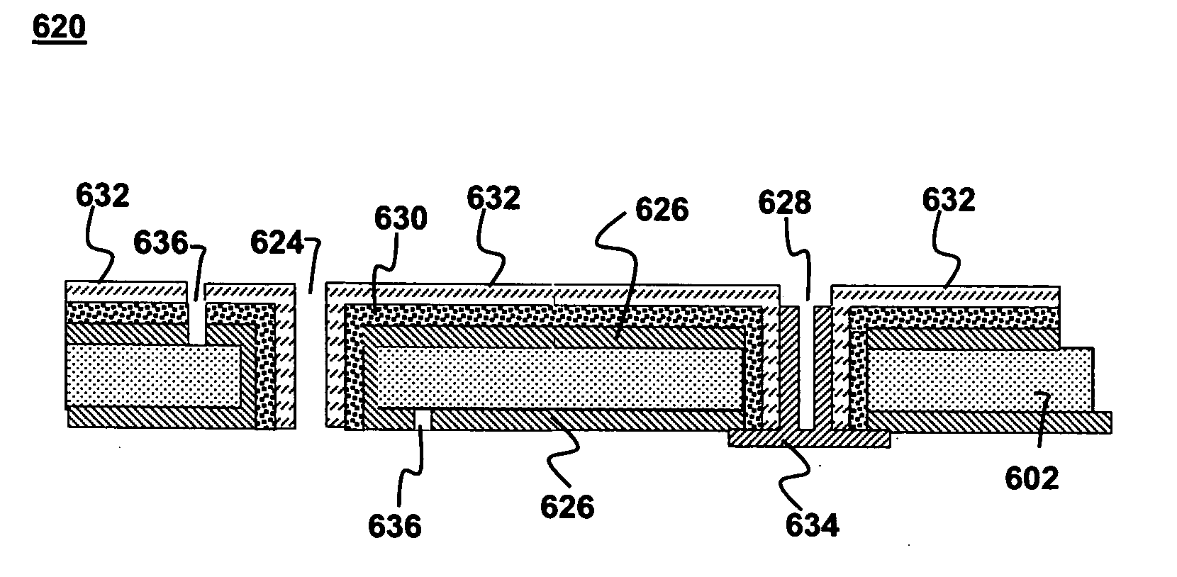
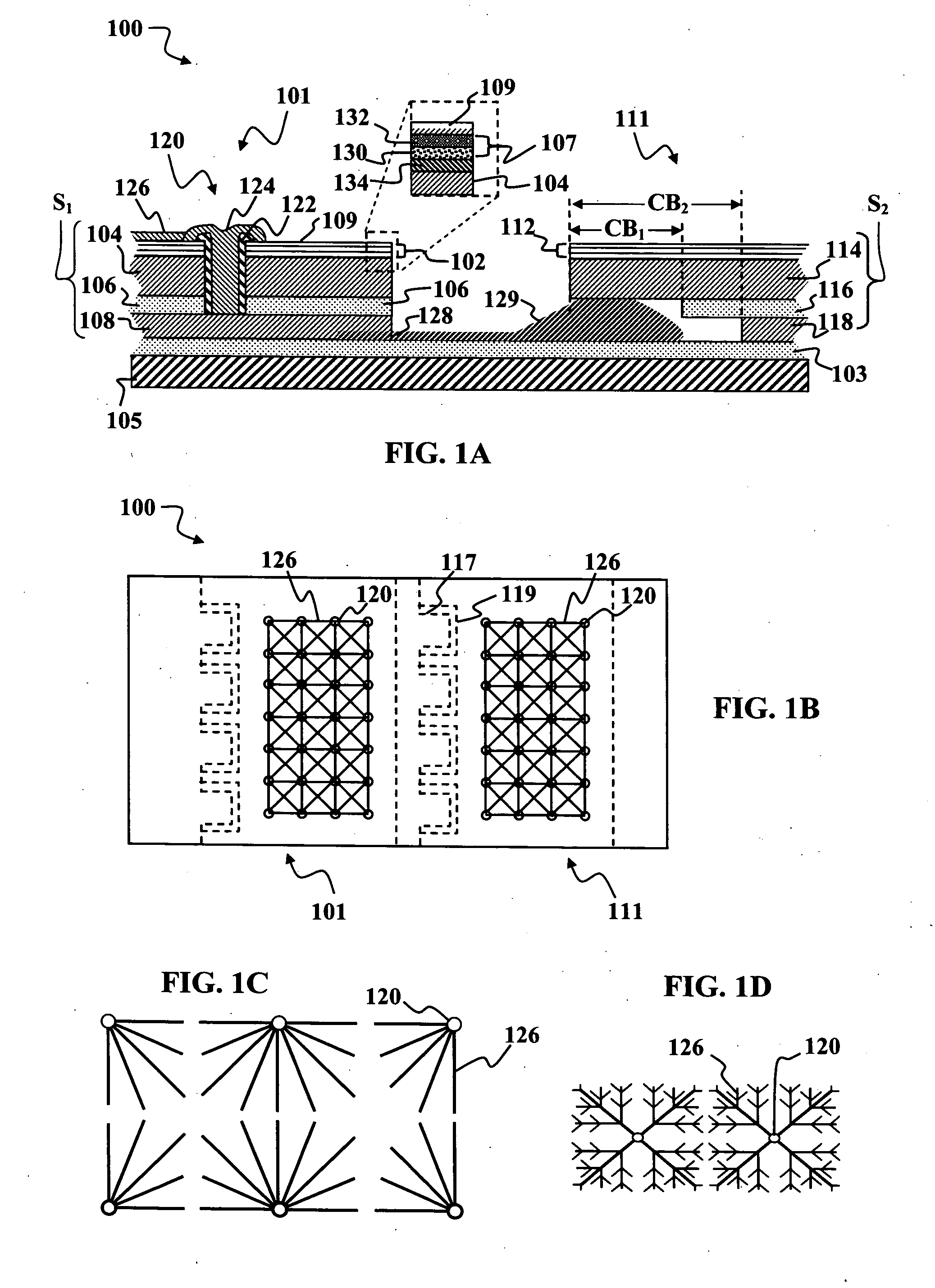
[0026]FIGS. 1A-1B illustrates an array 100 of optoelectronic devices according to an embodiment of the present invention. The array 100 includes a first device module 101 and a second device module 111. The device modules 101, 111 may be photovoltaic devices, such as solar cells, or light-emitting devices, such as light-emitting diodes. In a preferred embodiment, the device modules 101, 111 are solar cells. The first and second device modules 101, 111 are attached to an insulating carrier substrate 103, which may be made of a plastic mater...


PUM


Abstract

Optoelectronic device modules, arrays optoelectronic device modules and methods for fabricating optoelectronic device modules are disclosed. The device modules are made using a starting substrate having an insulator layer sandwiched between a bottom electrode made of a flexible bulk conductor and a conductive back plane. An active layer is disposed between the bottom electrode and a transparent conducting layer. One or more electrical contacts between the transparent conducting layer and the back plane are formed through the transparent conducting layer, the active layer, the flexible bulk conductor and the insulating layer. The electrical contacts are electrically isolated from the active layer, the bottom electrode and the insulating layer.

Description

OPTOELECTRONIC ARCHITECTURE HAVING COMPOUND CONDUCTING SUBSTRATE CROSS-REFERENCE TO RELATED APPLICATION [0001] This application is a continuation-in-part of commonly-assigned, co-pending application Ser. No. 11 / 039,053, filed Jan. 20, 2005, the entire disclosures of which are incorporated herein by reference. FIELD OF THE INVENTION [0002] This invention relates to optoelectronic devices and more particularly to mass-manufacture of optoelectronic devices such as solar cells. BACKGROUND OF THE INVENTION [0003] Optoelectronic devices can convert radiant energy into electrical energy or vice versa. These devices generally include an active layer sandwiched between two electrodes, sometimes referred to as the front and back electrodes, at least one of which is typically transparent. The active layer typically includes one or more semiconductor materials. In a light-emitting device, e.g., a light-emitting diode (LED), a voltage applied between the two electrodes causes a current to flow t...

Claims


Application Information

Patent Timeline
IPC IPC(8): H02N6/00
CPCH01L27/3204H01L31/0392H01L31/0749H01L31/046H01L51/5203Y02E10/541H01L31/18H01L31/0463H01L31/0465H01L31/03923H01L31/03925Y02P70/50H10K59/86H10K50/805
Inventor SHEATS, JAMES R.KAO, SAMROSCHEISEN, MARTIN R.
Owner AERIS CAPITAL SUSTAINABLE IP
Why Eureka
Try Eureka