Delay time correction circuit, video data processing circuit, and flat display device

a technology of delay time and correction circuit, applied in the direction of single output arrangement, pulse technique, instruments, etc., can solve the problems of image to be displayed may become visually remarkably undesirable, delay time becomes long in response, delay time varies, etc., to avoid variation in delay time, effective avoid various influences, effect of effective avoidance

Inactive Publication Date: 2006-07-27
JAPAN DISPLAY WEST
View PDF6 Cites 4 Cited by
  • Summary
  • Abstract
  • Description
  • Claims
  • Application Information

AI Technical Summary

Benefits of technology

[0018] According to the configuration of the present invention, it is possible to effectively avoid a variation in delay time in the logical circuit using TFTs or the like, so that it is possible to display a desired image while effectively avoiding various influences due to the variation in delay time.
[0019] According to the present invention, it is possible to provide a video data processing circuit and a flat display device both of which can effectively avoid a variation in delay time in a logical circuit using TFTs or the like.

Problems solved by technology

This kind of logical circuit using low-temperature polysilicon TFTs which is applied to the liquid crystal display device has the problem that if an input value is held at an L level for a long time, delay time becomes long in response at the rise of the following logical level, so that the delay time varies according to the length of the immediately preceding logical level.
Accordingly, there occurs a case where erroneous data may be latched as to only a particular bit of the gradation data, so that an image to be displayed may become visually remarkably undesirable.

Method used


Image

  • Delay time correction circuit, video data processing circuit, and flat display device
  • Delay time correction circuit, video data processing circuit, and flat display device
  • Delay time correction circuit, video data processing circuit, and flat display device

Examples


embodiment 1

[0041] (2) Configuration of Embodiment 1

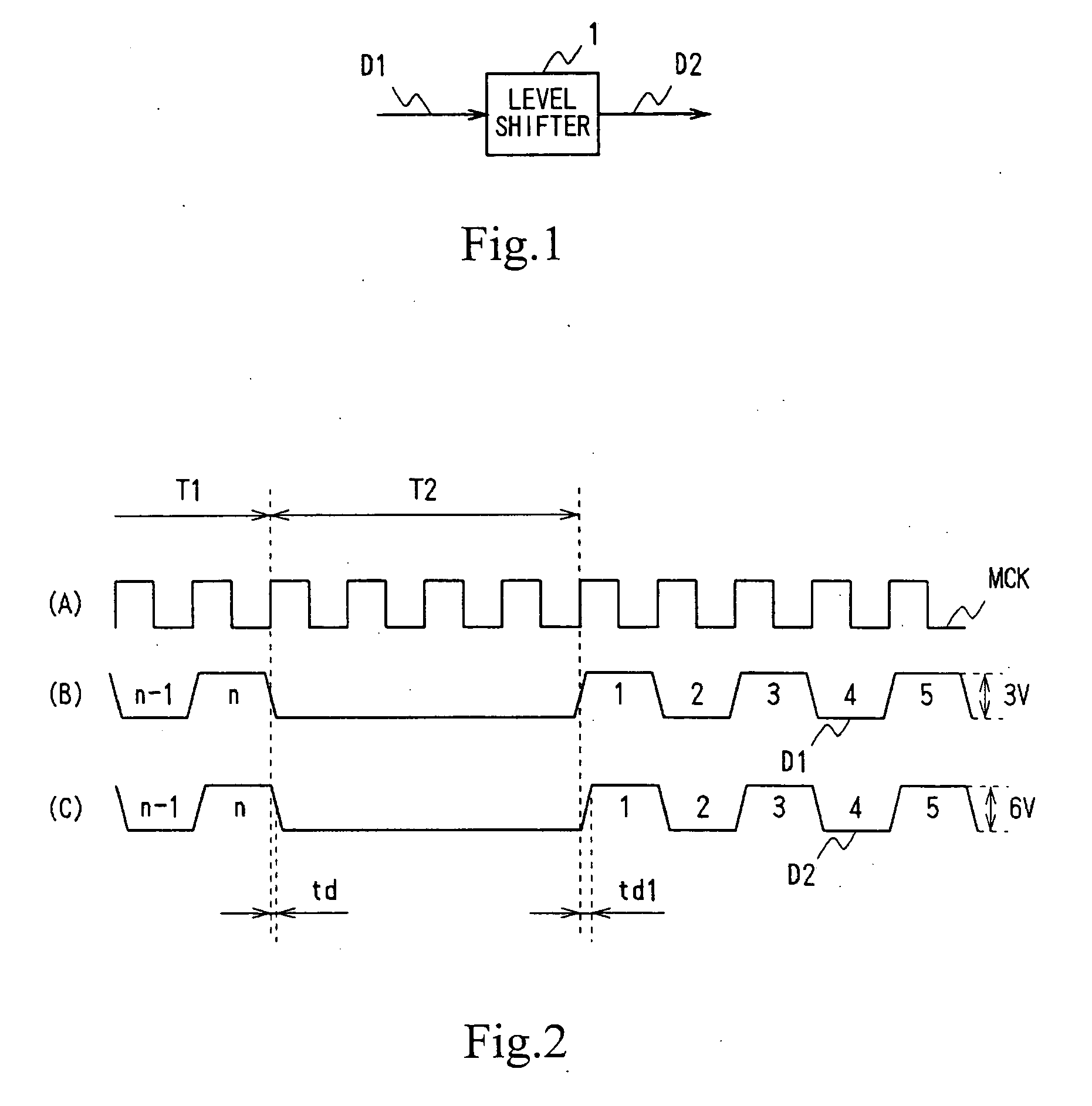
[0042]FIG. 8 is a block diagram showing a liquid crystal display device according to Embodiment 1 of the present invention. In a liquid crystal display device 11, the driving circuits shown in FIG. 8 are integrally formed on a glass substrate which is an insulating substrate of a display section 12, and driving circuits which will be described later, such as horizontal driving circuits and a timing generator, are formed by TFTs made of low-temperature polysilicon.

[0043] The display section 12 has pixels each formed by a liquid crystal cell, a TFT which is a switching device for the liquid crystal cell, and a storage capacitor, and has a rectangular shape in which these pixels are arranged in a matrix form.

[0044] A vertical driving circuit 13 drives gate lines of the display section 12 in response to various timing signals outputted from a timing generator 14, thereby sequentially selecting the pixels provided in the display section 12, in un...

embodiment 2

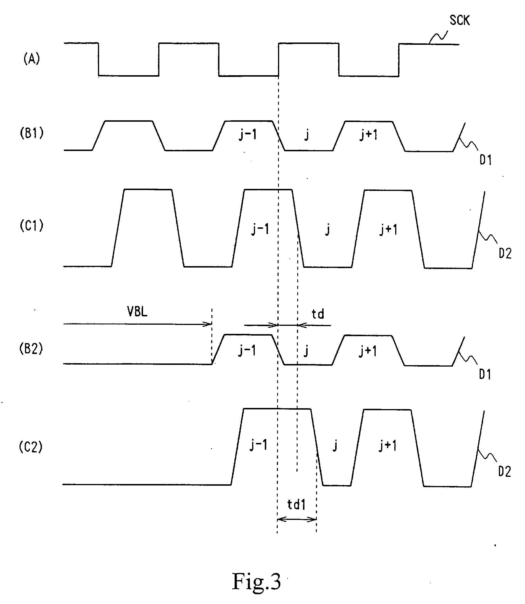
[0066] (5) Embodiment 2

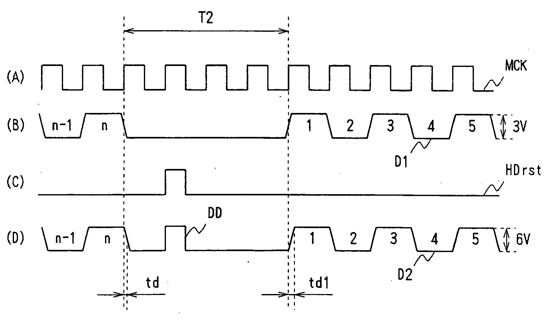
[0067] The above-mentioned embodiment 1 is configured to insert dummy data during a horizontal blanking period and prevent an increase in delay time associated with the fall of logical level following the horizontal blanking period, on the basis of the view that it is possible to prevent a variation in delay time in a logical circuit using TFTs or the like by inserting dummy data during a quiescent period.

[0068] Contrarily, as mentioned in connection with the delay time correction principle, as to the rise of logical level in the logical circuit using TFTs, oppositely to the case of the fall of logical level, with a configuration in which when the logical level of input data is held at a constant value for a constant period immediately before the rise, delay time decreases and dummy data is inserted during a quiescent period, it is possible to prevent a variation in delay time associated with such decrease in delay time.

[0069] In order to verify the advantag...


PUM


Abstract

The present invention is applied to, for example, a liquid crystal display device having a driving circuit integrally formed on an insulating substrate, and makes it possible to effectively avoid a variation in delay time in a logical circuit using TFTs or the like by inserting dummy data (DD) into input data (D1) and forcedly switching the logical level of the input data (D1) at a predetermined timing during a quiescent period (T2) in which the input data is held at a constant logical level.

Description

BACKGROUND OF THE INVENTION [0001] 1. Technical Field [0002] The present invention relates to a delay time correction circuit, a video data processing circuit, and a flat display device, and can be applied to, for example, a liquid crystal display device having a driving circuit integrally formed on an insulating substrate. The present invention makes it possible to effectively avoid a variation in delay time in a logical circuit using TFTs or the like by inserting dummy data into input data and forcedly switching the logical level of the input data. [0003] 2. Background Art [0004] In recent years, a liquid crystal display device of the type in which a driving circuit for a liquid crystal display panel is integrally integrated and configured on a glass substrate which is an insulating substrate constituting part of the liquid crystal display panel has been provided as a liquid crystal display device which is a flat display device applied to mobile terminals such as mobile phones and...

Claims


Application Information

Patent Timeline
Patent Type & Authority Applications(United States)
IPC IPC(8): G09G3/36H03K3/356H03K5/13H03K19/0185
CPCG09G2300/0408G09G3/3685G09G3/20G09G3/36
Inventor MURASE, MASAKINAKAJIMA, YOSHIHARUKIDA, YOSHITOSHI
Owner JAPAN DISPLAY WEST
Why Eureka
Try Eureka