

Active matrix substrate and its manufacturing method
- Summary
- Abstract
- Description
- Claims
- Application Information
AI Technical Summary
Benefits of technology
Problems solved by technology
Method used
Image

Examples
first preferred embodiment
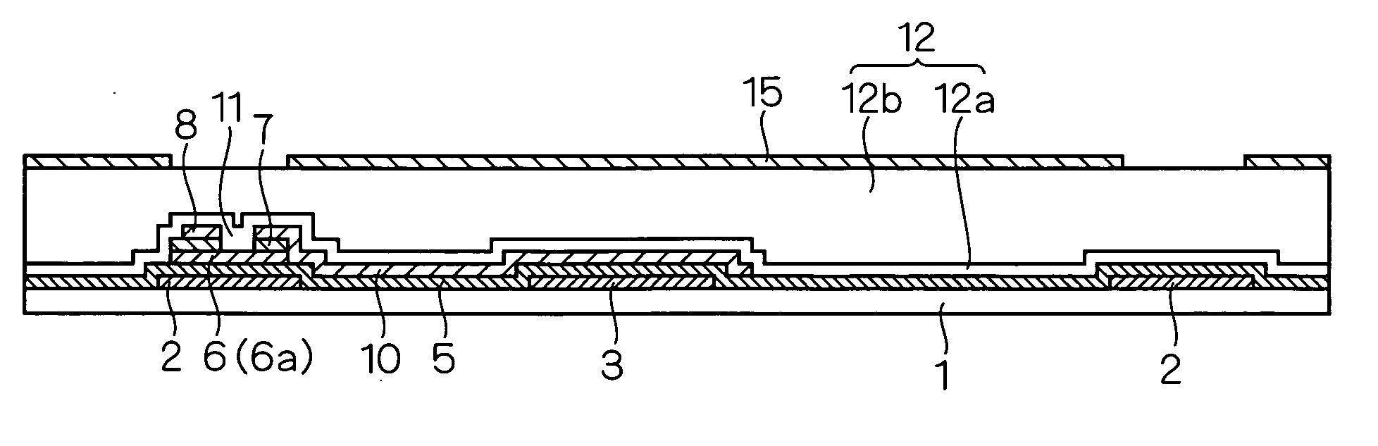
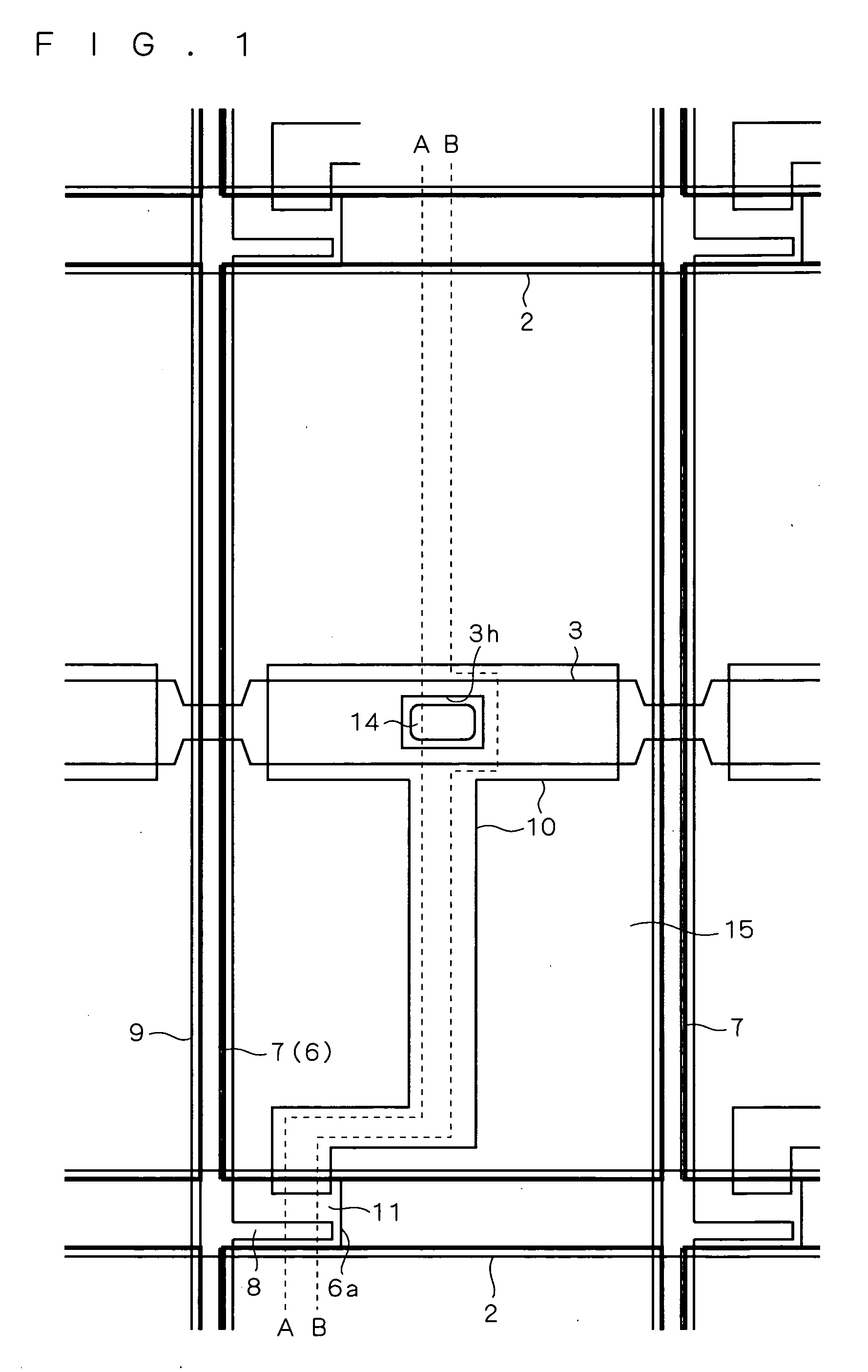
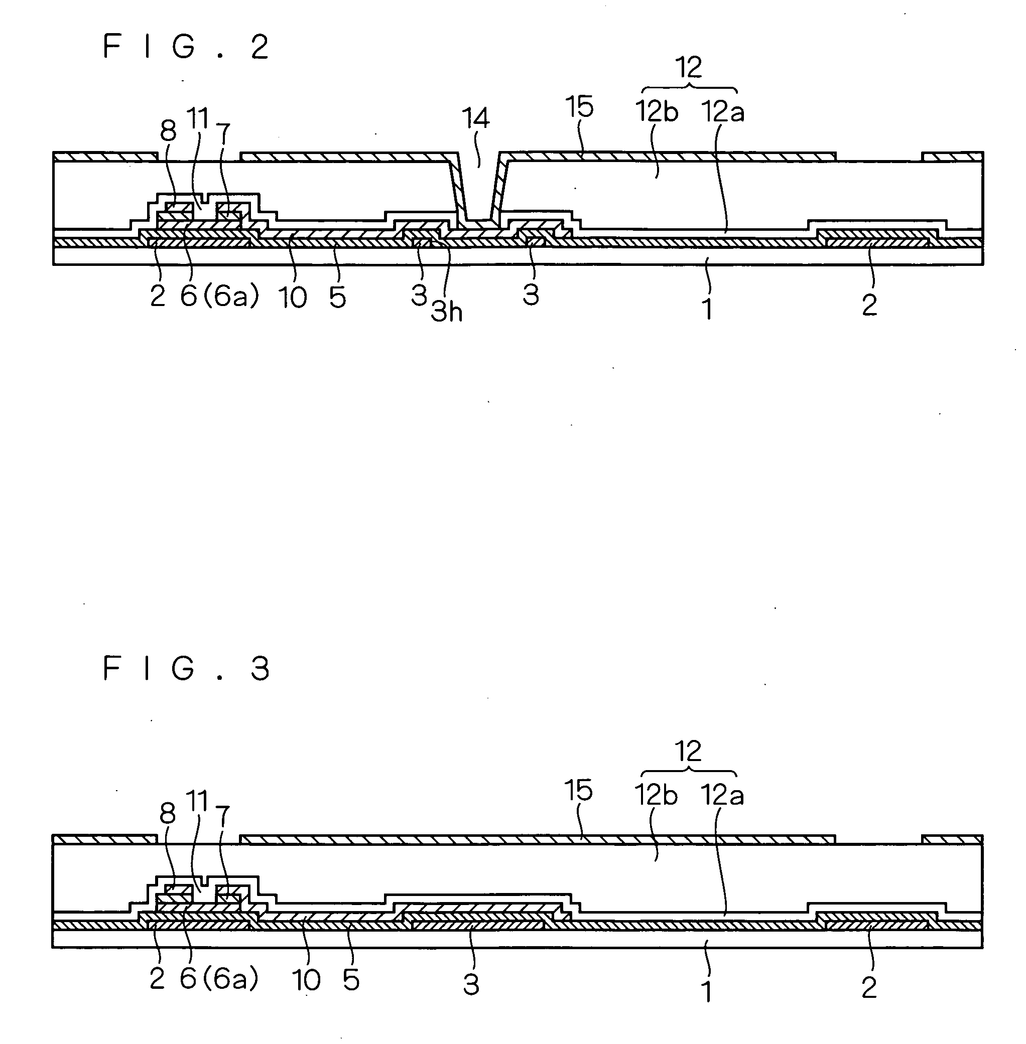
[0030] Now, an active matrix substrate according to a first preferred embodiment of the present invention will be described. This preferred embodiment describes an active matrix substrate for use in transmissive liquid crystal displays.
[0031]FIG. 1 is a plan view of an active matrix substrate; FIG. 2 is a cross-sectional view taken along line A-A of FIG. 1; and FIG. 3 is a cross-sectional view taken along line B-B of FIG. 1.
[0032] In this active matrix substrate, a plurality of gate lines 2 (scanning lines) and a plurality of auxiliary capacitive electrodes 3 are formed on a transparent insulated substrate 1 (cf. FIGS. 4 and 9A). The plurality of gate lines 2 are formed in straight lines and spaced at appropriate intervals to extend approximately parallel to each other on the transparent insulated substrate 1. Portions of the gate lines 2 on which a semiconductor film 6 to be described later is formed serve as gate electrodes of thin-film transistors.
[0033] Each of the auxiliary ...
second preferred embodiment
[0073] Now, an active matrix substrate according to a second preferred embodiment of the present invention will be described. This preferred embodiment describes an active matrix substrate for use in semitransparent liquid crystal displays.
[0074]FIG. 12 is a plan view of an active matrix substrate; FIG. 13 is a cross-sectional view taken along line C-C of FIG. 12; and FIG. 14 is a cross-sectional view taken along line D-D of FIG. 12.
[0075] The following is a description of main differences of the active matrix substrate according to this second preferred embodiment from the one according to the first preferred embodiment. Here, components identical to those according to the aforementioned first preferred embodiment are denoted by the same reference numerals, which will not be described in detail.
[0076] While in the first preferred embodiment, the pixel electrodes 15 are formed of only a transparent conductive film, pixel electrode sections for pixel display in the second preferre...
PUM
 Abstract
Description
Claims
Application Information