Low power chip select (CS) latency option

a low-power, clock-selecting technology, applied in the field of electronic devices, can solve the problems of inability to apply valid executable commands one or more clock cycles, inability to apply valid executable commands at any time, and inability to meet the requirements of a single clock cycl

Inactive Publication Date: 2006-08-10
ROUND ROCK RES LLC
View PDF10 Cites 136 Cited by
  • Summary
  • Abstract
  • Description
  • Claims
  • Application Information

AI Technical Summary

Benefits of technology

[0019] According to a system and method of the present disclosure, the standby currents in input buffers in an electronic device (e.g., a memory device) are reduced when the input buffers may be activated or deactivated by the state of a chip select (CS) signal. In case of a memory device, the active and precharge standby currents in memory input buffers may be reduced by turning off the input buffers when the CS signal is in an inactive state. A memory controller may supply the CS signal to the memory device at least one clock cycle earlier than other control signals including the RAS (row address strob

Problems solved by technology

This current consumption may be unnecessary especially when the memory row is in a standby mode after being activated or precharged, i.e., during the time when no data read/write operations are actually taking

Method used


Image

  • Low power chip select (CS) latency option
  • Low power chip select (CS) latency option
  • Low power chip select (CS) latency option

Examples


Embodiment Construction

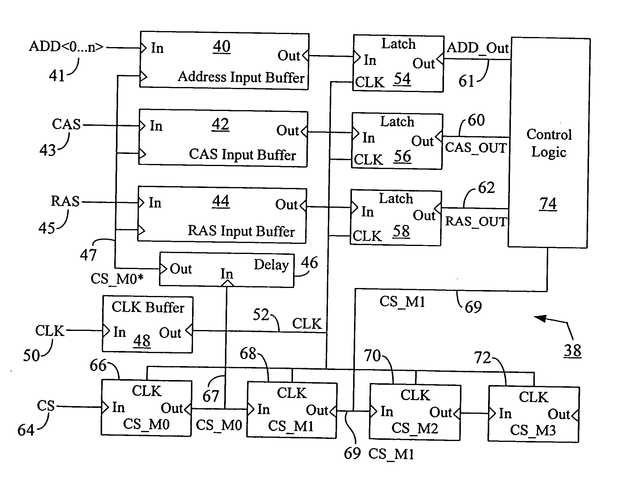
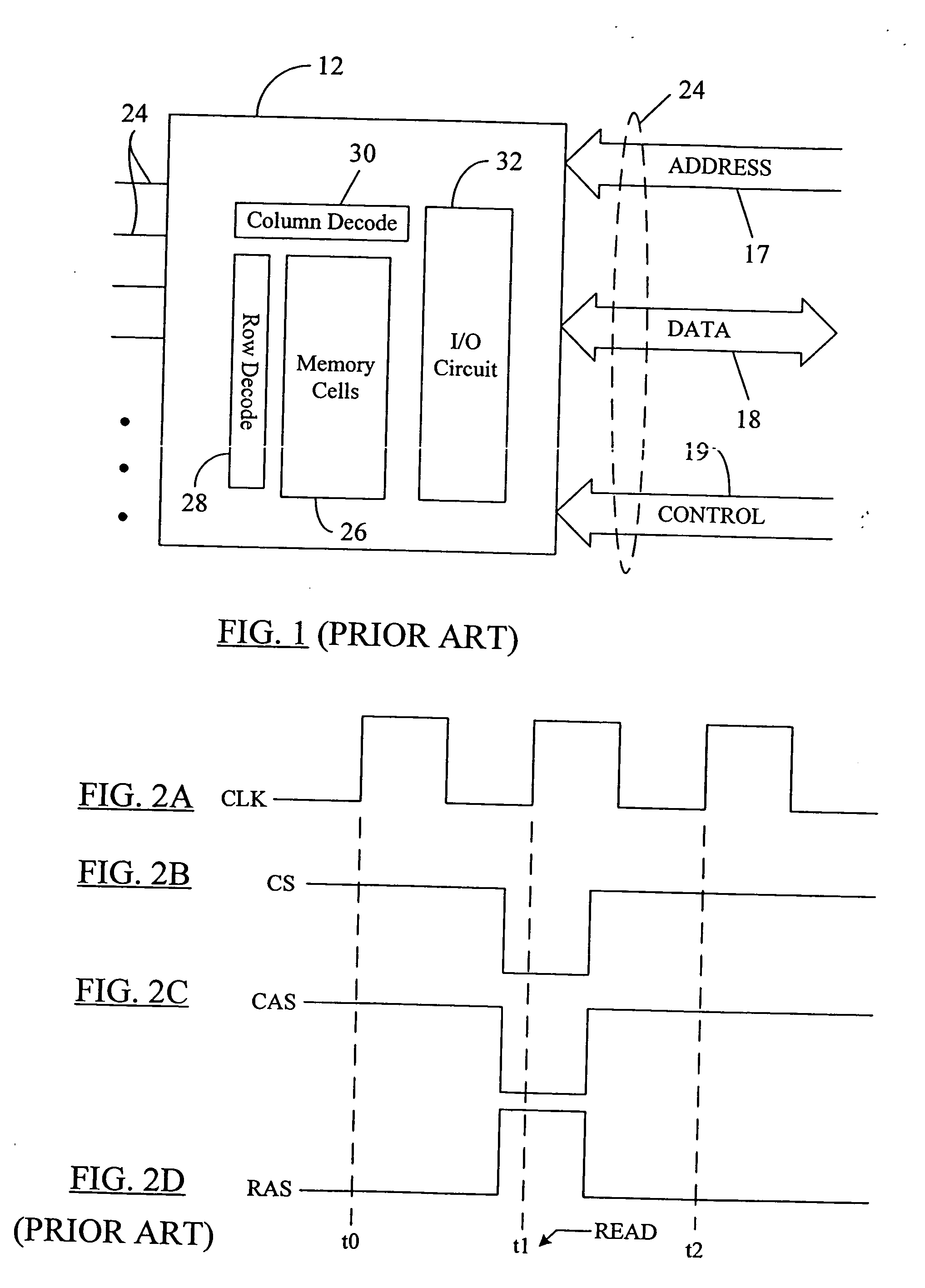
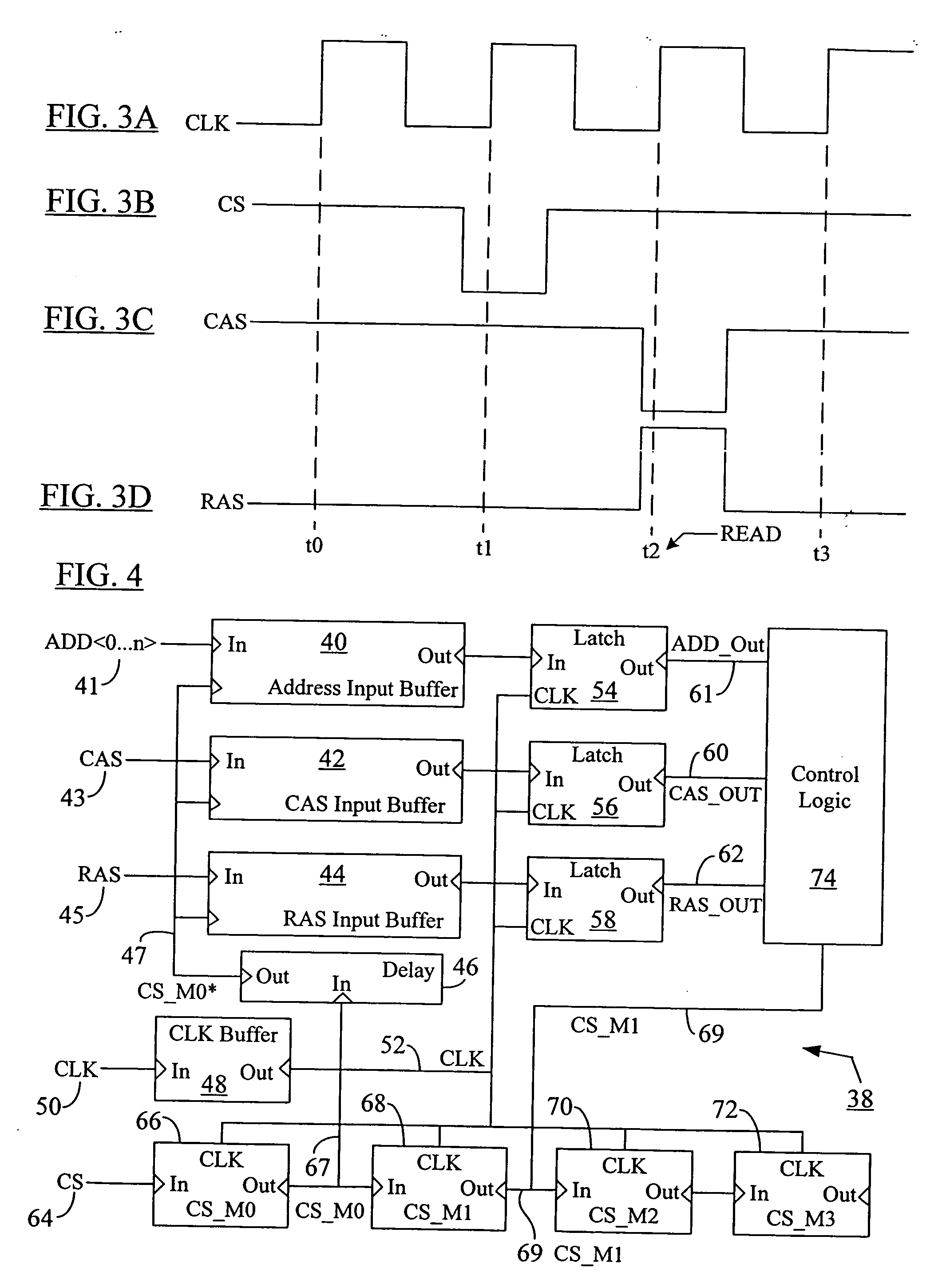
[0029] Reference will now be made in detail to certain embodiments of the present disclosure, examples of which are illustrated in the accompanying drawings. It is to be understood that the figures and descriptions of the present disclosure included herein illustrate and describe elements that are of particular relevance to the present disclosure, while eliminating, for the sake of clarity, other elements found in typical solid-state electronic devices, memories or memory-based systems. It is noted at the outset that the terms “connected”, “connecting,”“electrically connected,” etc., are used interchangeably herein to generally refer to the condition of being electrically connected. It is further noted that various block diagrams and circuit diagrams shown and discussed herein employ logic circuits that implement positive logic, i.e., a high value on a signal is treated as a logic “1” whereas a low value is treated as a logic “0.” However, any of the circuits discussed herein may be...


PUM


Abstract

A system and method to reduce standby currents in input buffers in an electronic device (e.g., a memory device) is disclosed. The input buffers may be activated or deactivated by the state of a chip select (CS) signal. In case of a memory device, the active and precharge standby currents in memory input buffers may be reduced by turning off the input buffers when the CS signal is in an inactive state. A memory controller may supply the CS signal to the memory device at least one clock cycle earlier than other control signals including the RAS (row address strobe) signal, the CAS (column address strobe) signal, the WE (write enable) signal, etc. A modified I/O circuit in the memory device may internally delay the CS signal by at least one clock cycle to coincide its timing with the RAS/CAS signals for normal data access operation whereas the turning on/off of the memory input buffers may be performed by the CS signal received from the memory controller on the previous cycle. Thus, activation and deactivation of memory input buffers may be performed without forcing the memory device into power down mode and without employing complex circuits for power management. Because of the rules governing abstracts, this abstract should not be used to construe the claims.

Description

BACKGROUND [0001] 1. Field of the Disclosure [0002] The present disclosure generally relates to electronic devices and, more particularly, to a system and method to reduce current consumption in semiconductor memory chips. [0003] 2. Brief Description of Related Art [0004] Memory devices are electronic devices that are widely used in many electronic products and computers to store data. A memory device is a semiconductor electronic device that includes a number of memory cells, each cell storing one bit of data. The data stored in the memory cells can be read during a read operation. FIG. 1 is a simplified block diagram showing a memory chip or memory device 12. The memory chip 12 may be part of a DIMM (dual in-line memory module) or a PCB (printed circuit board) containing many such memory chips (not shown in FIG. 1). The memory chip 12 may include a plurality of pins or ball contacts 24 located outside of chip 12 for electrically connecting the chip 12 to other system devices. Some...

Claims


Application Information

Patent Timeline
IPC IPC(8): G11C7/00
CPCG11C7/1078G11C7/109G11C7/20G11C2211/4067
Inventor STAVE, ERIC
Owner ROUND ROCK RES LLC
Why Eureka
Try Eureka