

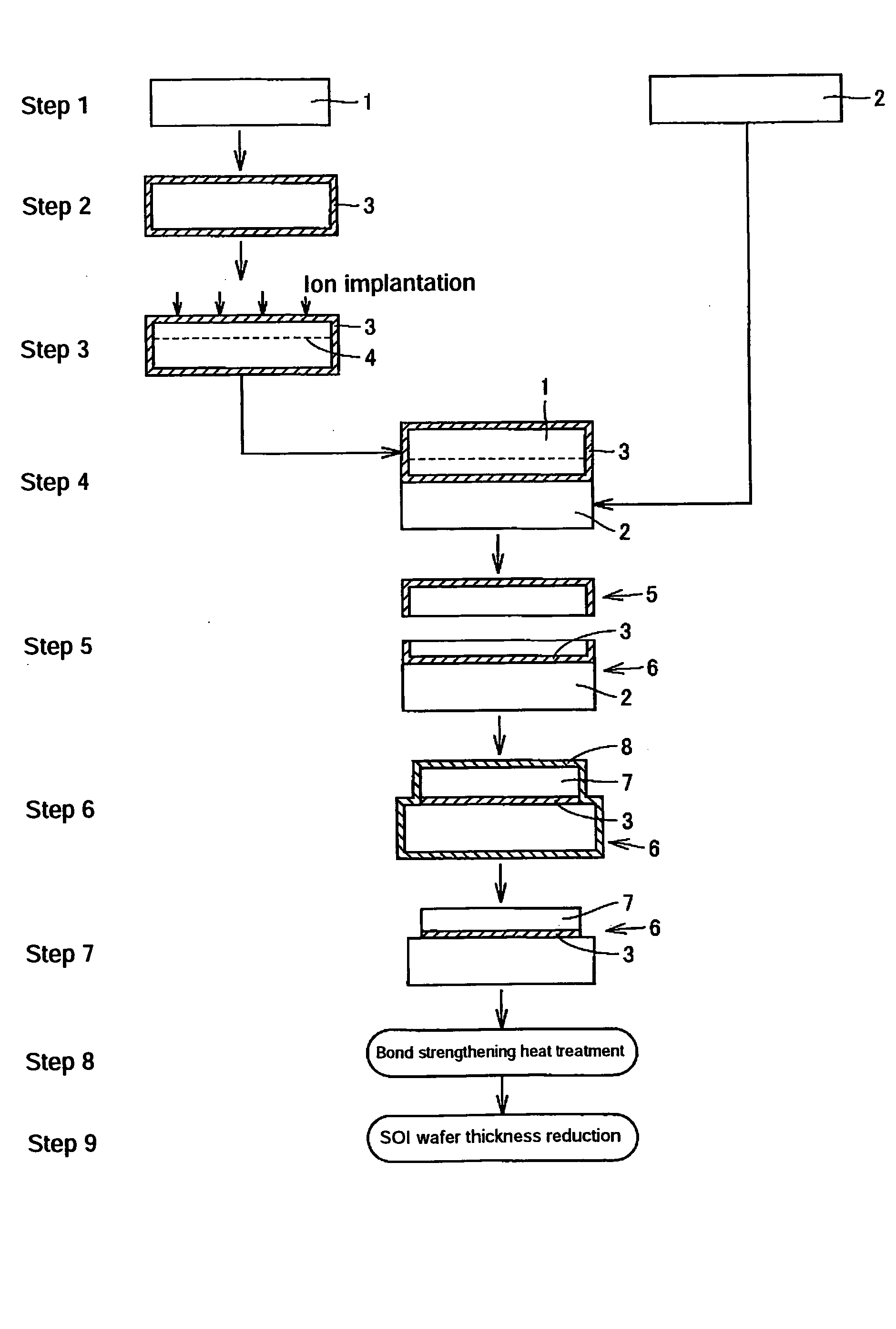
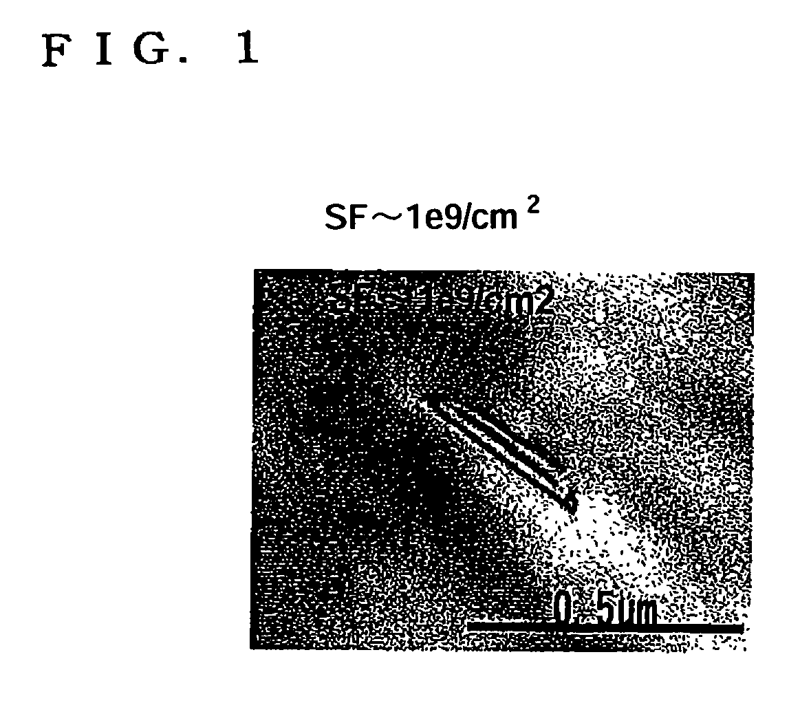
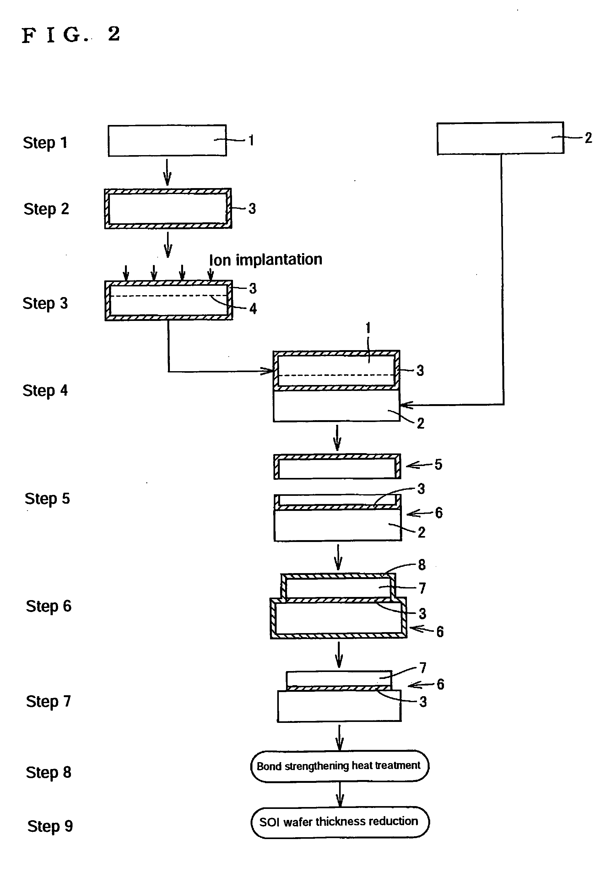
SOI wafer production method
a production method and technology of soi wafer, applied in the direction of semiconductor/solid-state device manufacturing, basic electric elements, electric apparatus, etc., can solve the problems of forming stacking faults and stacking faults by interstitial silicon atoms that have agglomeration, and achieve the effect of facilitating the reduction deteriorating the uniformity of soi layer thickness
- Summary
- Abstract
- Description
- Claims
- Application Information
AI Technical Summary
Benefits of technology
Problems solved by technology
Method used
Image

Examples
examples
[0049] In Inventive Examples, wafers, 200 mm in diameter, were cut out of respective silicon single crystal ingots produced by doping with C by the Czochralski process, showing p type conductivity and having a resistivity of 1-20 Ω·cm, and then mirror-polished. Each C-doped single crystal was produced by pulling up a single crystal from a silicon melt doped with a predetermined amount of a C powder.
[0050] The wafers thus obtained respectively had three levels of C concentration, namely 1×10¹⁶ atoms / cm3, 5×10¹⁶ atoms / cm3 and 1×10¹⁷ atoms / cm3, and had an oxygen concentration of 8×10¹⁷ atoms / cm3 to 14×1017 atoms / cm3. These were divided into active layer wafers and base wafers. The C concentration was confirmed by infrared absorption spectrometry (IR absorption).
[0051] In Comparative Example 1, mirror surface silicon wafers, 200 mm in diameter, produced without C doping, showing p type conductivity and having a resistivity of 1-20 Ω·cm were used, and wafers having an oxygen concentrat...
PUM
 Abstract
Description
Claims
Application Information