

Manufacturing method for semiconductor device and rapid thermal annealing apparatus
a manufacturing method and technology of semiconductor devices, applied in semiconductor devices, electrical equipment, semiconductor/solid-state device testing/measurement, etc., can solve the problems of reducing the yield of semiconductor devices, affecting the and reducing reliability, so as to minimize the inconsistency of electrical properties of semiconductor devices and minimize the inconsistency of electrical properties within a wafer surfa
- Summary
- Abstract
- Description
- Claims
- Application Information
AI Technical Summary
Benefits of technology
Problems solved by technology
Method used
Image

Examples
first embodiment
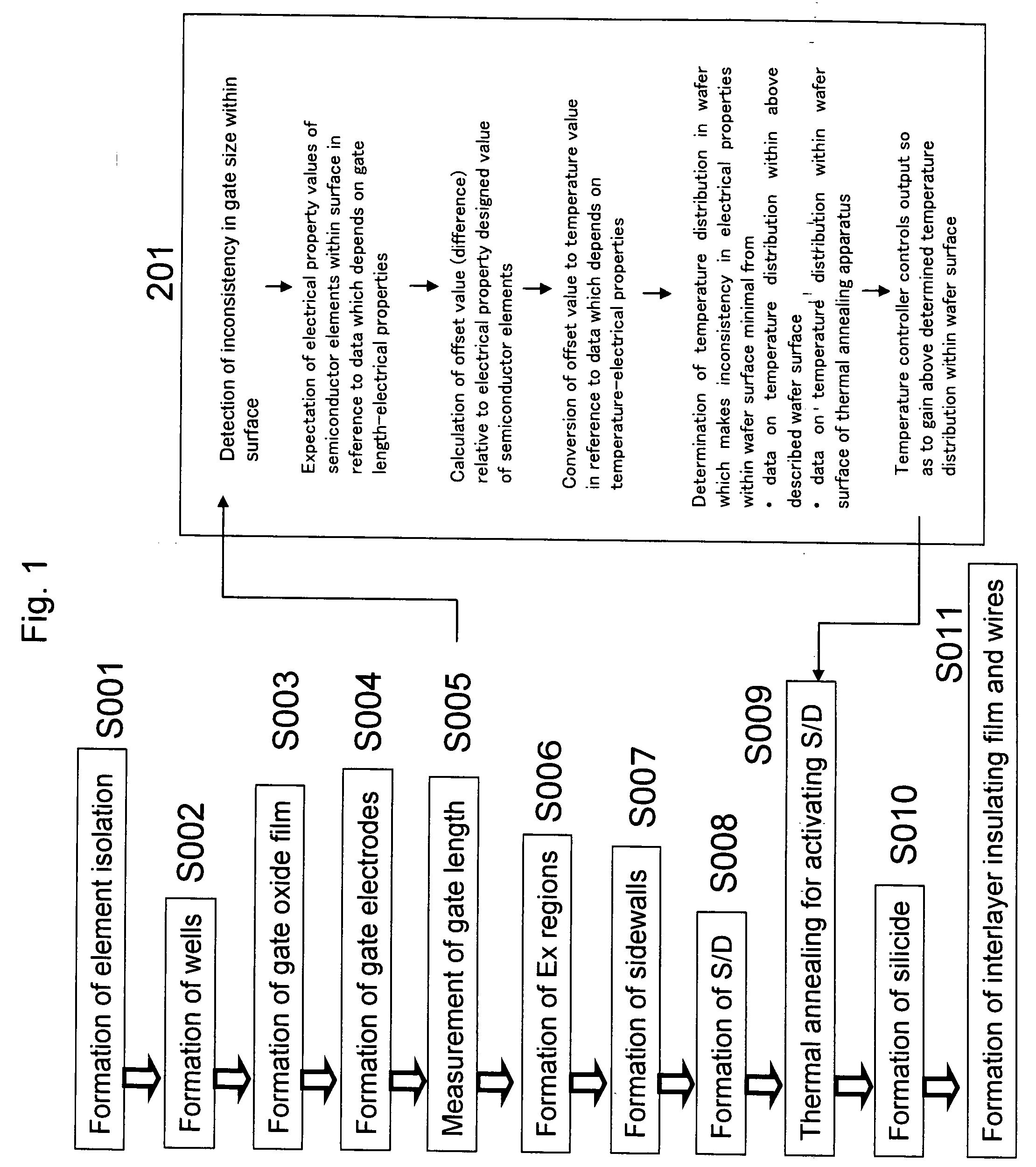
[0040] In the following, an embodiment of the present invention is described in reference to FIGS. 1, 2A to 2C, 3, 4, 5 and 6.
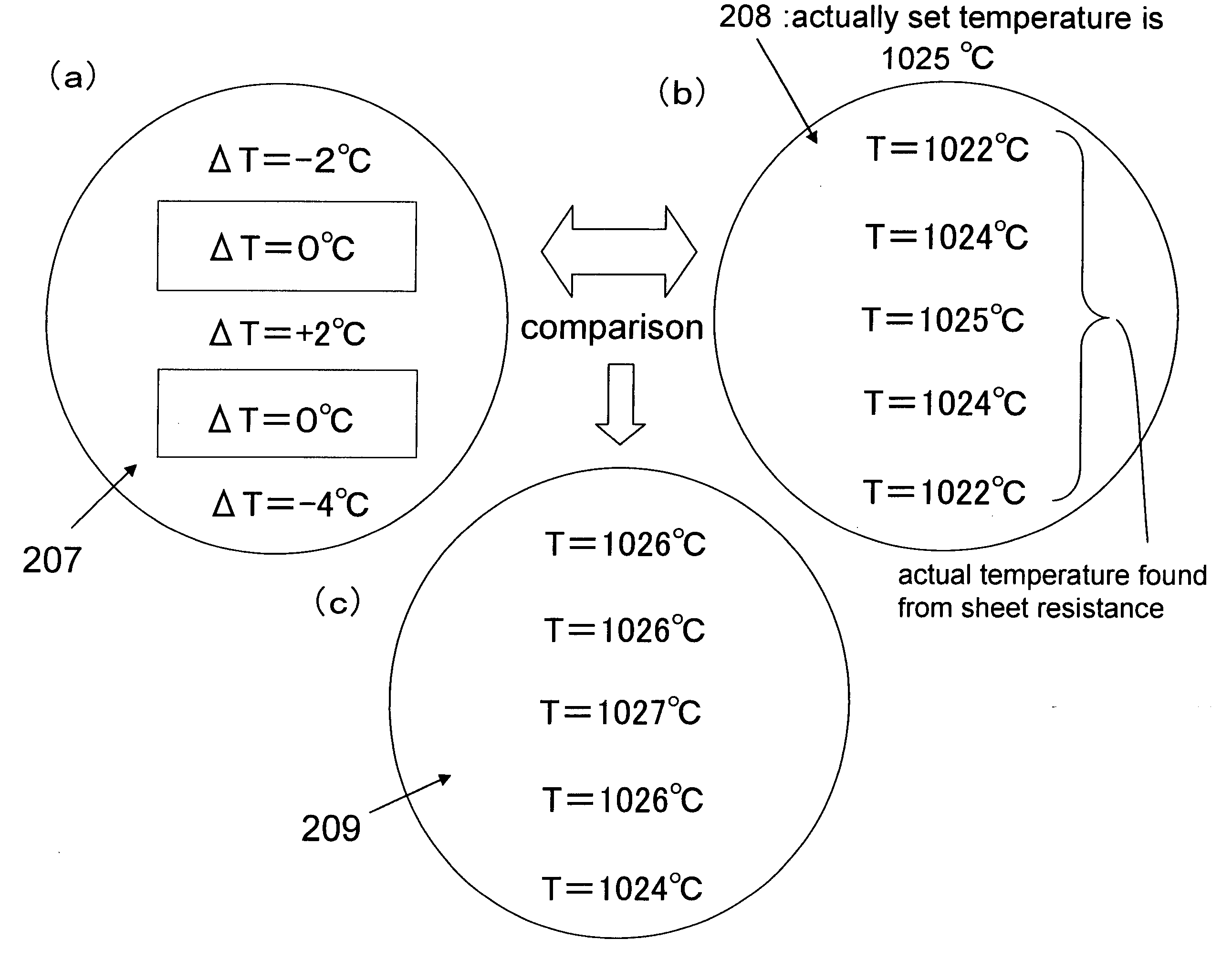
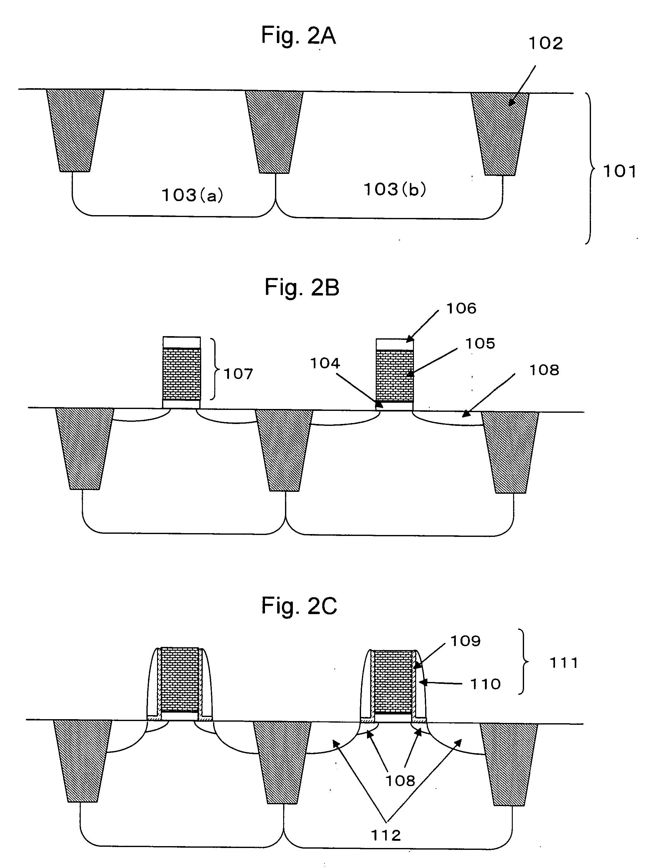
[0041]FIG. 1 is a flow chart illustrating a manufacturing method for a semiconductor device according to the present invention. FIGS. 2A, 2B and 2C are cross sectional diagrams illustrating the manufacturing steps for a semiconductor device. FIG. 3 is a diagram illustrating a method for converting distribution in the gate size within a surface that has been gained in Step S005 into distribution in the electrical properties of the semiconductor device within a surface. FIG. 4 is a diagram illustrating data on distribution in the difference between the electrical property values of the semiconductor device and the designed values within a surface. FIG. 5 is a diagram illustrating a method for converting data on distribution in the difference between the electrical property values of the semiconductor device and the designed values within a surface into distrib...
second embodiment
[0064] In the following, an embodiment of the present invention is described in reference to FIG. 7.
[0065]FIG. 7 is a flow chart illustrating another manufacturing method for a semiconductor device according to the present invention.
[0066] This embodiment is different from the first embodiment in that electrical measurement is inserted as Step S010# after the formation of silicide in Step S010, so that the results of measurement can be fed back to data 208 on the temperature distribution within the wafer surface in the equipment.
[0067] In the present step, the electrical properties of semiconductor elements are measured using a scribe PCM (press control monitor) pattern that is provided in order to confirm how the elements are made. Inconsistency in the electrical properties gained herein within the wafer surface corresponds only to inconsistency in the temperature of the thermal annealing apparatus in the case where the first embodiment is completely implemented. Therefore, the ...
third embodiment
[0069] In the following, another embodiment of the present invention is described in reference to FIG. 8.
[0070]FIG. 8 is a flow chart illustrating a manufacturing method for a semiconductor device according to the present invention.
[0071] This embodiment is different from the first embodiment in that the difference between the highest temperature and the lowest temperature within the wafer surface is calculated after the calculation of temperature distribution 209 within the wafer surface, and when this difference exceeds a certain value (20° C. in the present embodiment), an alarm indicating an abnormality in the process is generated at this point in time.
[0072] If this alarm is issued, it can be assumed that some abnormality has occurred anywhere between Step S001 to Step S009, or an abnormality (deterioration of a lamp or the like) has occurred in the thermal annealing apparatus. As described above, it becomes possible to detect abnormalities in the process which are not notic...
PUM
 Abstract
Description
Claims
Application Information