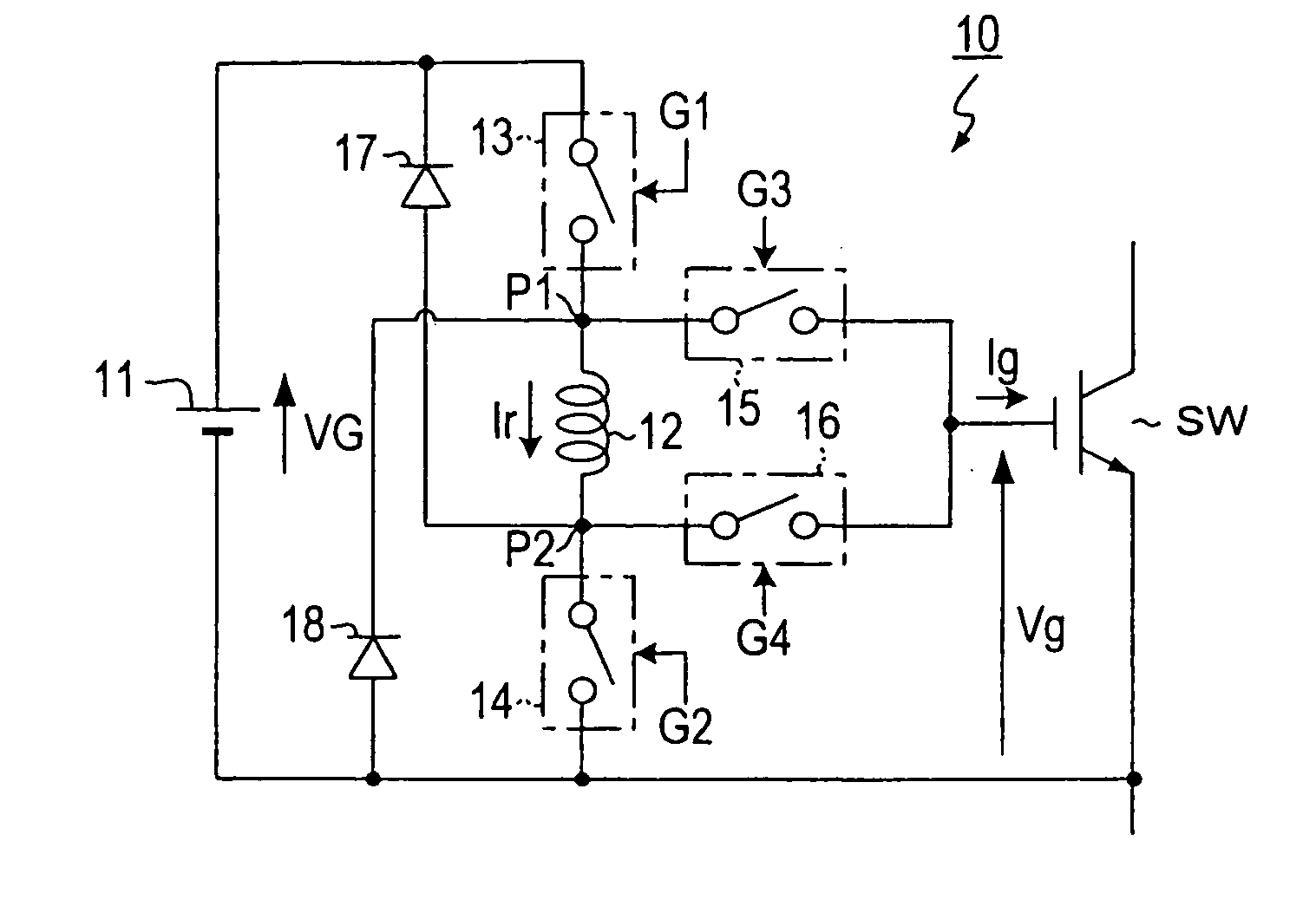
Gate driving circuit
a driving circuit and gate technology, applied in the direction of pulse technique, oscillation generator, power conversion system, etc., can solve the problems of increasing switching loss, short time required for charging/discharging the parasitic capacitance of the gate, and large current variation rate of the gate current, so as to reduce noise, reduce switching loss, and not quickly change the magnitude of the current
- Summary
- Abstract
- Description
- Claims
- Application Information
AI Technical Summary
Benefits of technology
Problems solved by technology
Method used
Image

Examples
first embodiment
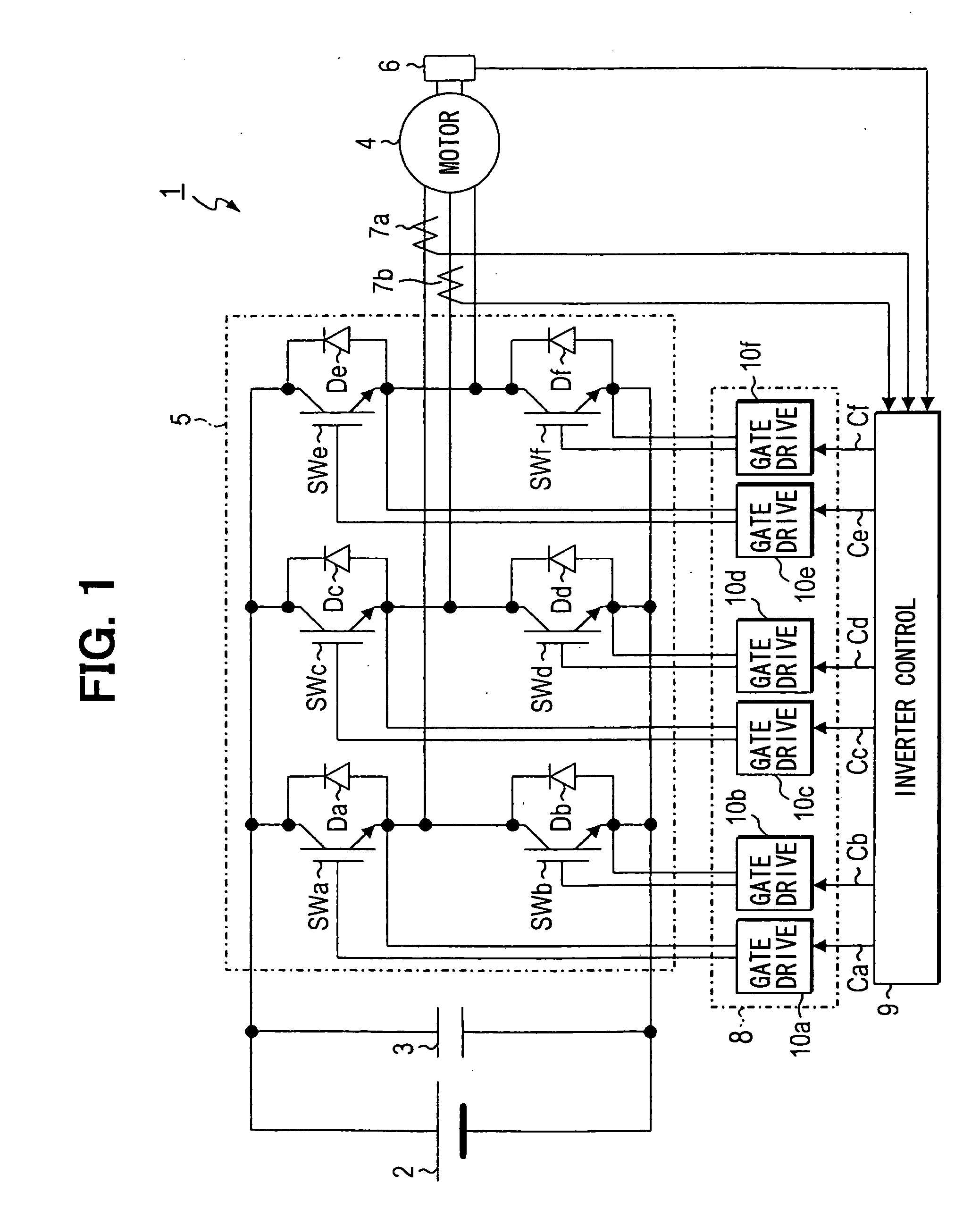
[0039] Referring first to FIG. 1, an inverter apparatus 1 includes a chargeable / dischargeable DC power source 2, a capacitor 3 connected in parallel to the DC power source 2 for smoothing a main current flowing through a power source line, an electric motor 4 as a load, and a three-phase bridge circuit 5 for receiving electric power from the DC power source 2 through the power source line and supplying currents to windings of respective phases U, V and W of the motor 4.
[0040] The three-phase bridge circuit 5 includes six switching devices SWa to SWf (collectively SW), and has a well-known structure in which three pairs, each including a pair of series-connected switching devices SW, are connected in parallel between the positive electrode and negative electrode of the DC power source 2. Connection portions of the switching devices SW of the respective pairs are connected to the windings of the respective phases U, V and W of the motor 4. An insulated gate bipolar transistor (IGBT) ...
second embodiment
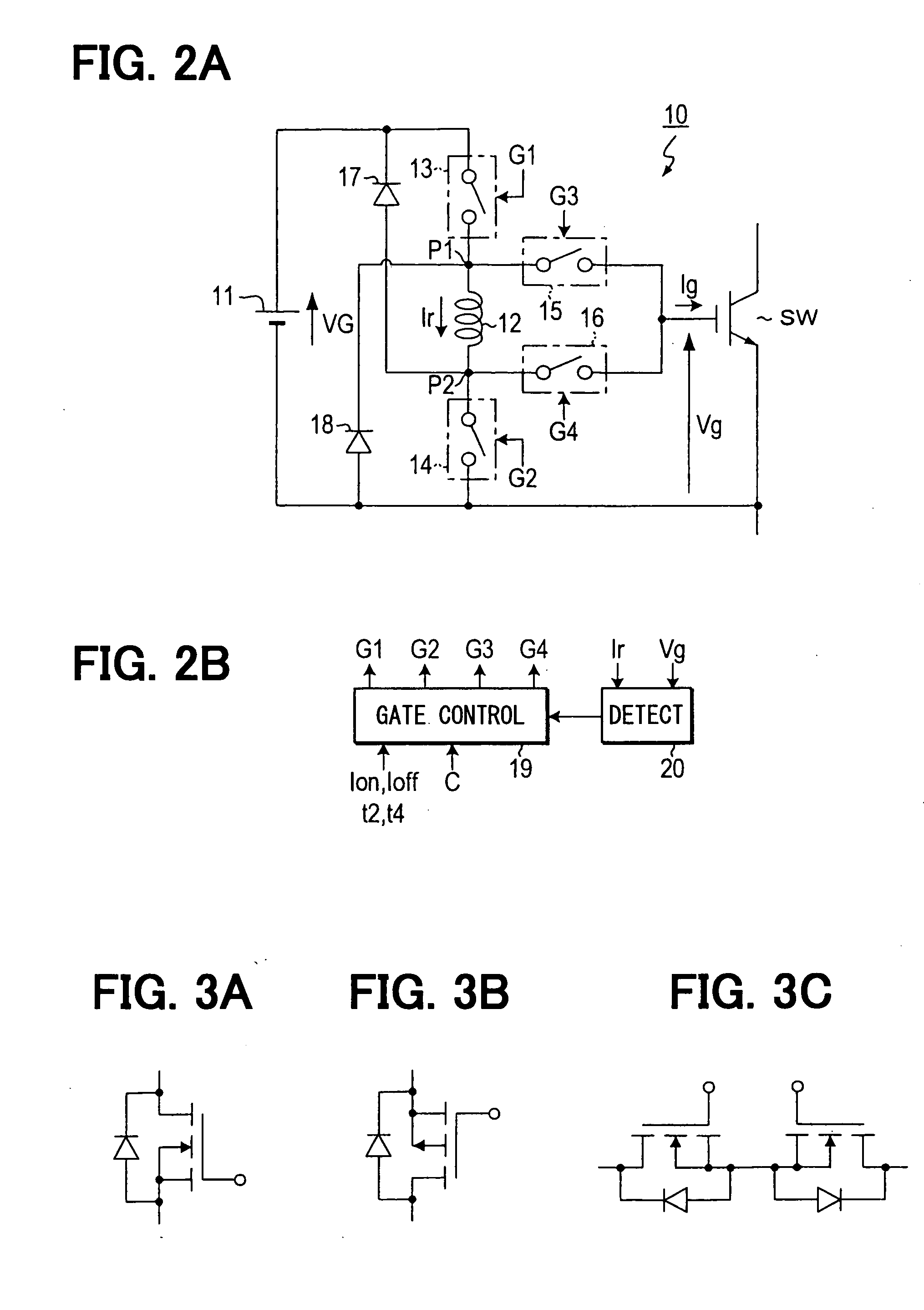
[0094] In the second embodiment, only a part of a gate driving circuit is different. As shown in FIG. 9A, a gate driving circuit 30 is similar to that of the first embodiment except that a pair of series-connected DC power sources 21 and 22 are used instead of the single DC current11, and a connection point (power source intermediate point) of both DC power sources 21 and 22 is connected to the emitter of the driving target device SW and is made to have a reference potential of the gate voltage.
[0095] The operation is similar to that of the first embodiment except that as shown in FIG. 5B, when the driving target device SW is turned off, an OFF-voltage applied to the gate is not 0 V but −VG.
[0096] In the gate driving circuit 30 constructed as stated above, when the driving target device SW is turned off, the negative voltage −VG is applied, and as compared with the case of the first embodiment, the charging / discharging speed of the gate capacitance is improved, so that the switchi...
PUM
 Abstract
Description
Claims
Application Information
 - R&D
- Intellectual Property
- Life Sciences
- Materials
- Tech Scout
- Unparalleled Data Quality
- Higher Quality Content
- 60% Fewer Hallucinations
Browse by: Latest US Patents, China's latest patents, Technical Efficacy Thesaurus, Application Domain, Technology Topic, Popular Technical Reports.
© 2025 PatSnap. All rights reserved.Legal|Privacy policy|Modern Slavery Act Transparency Statement|Sitemap|About US| Contact US: help@patsnap.com