High density plasma CVD chamber

a plasma cvd and high density technology, applied in the field of semiconductor processing equipment, can solve the problems of inefficient plasma coupling, center peaked or cusped plasma profiles, and difficult to establish a uniform plasma density over the entire substrate surface during processing, so as to reduce or minimize temperature fluctuations, improve particle performance, and improve the effect of temperature control of the upper chamber

Inactive Publication Date: 2006-08-31
APPLIED MATERIALS INC
View PDF11 Cites 34 Cited by
  • Summary
  • Abstract
  • Description
  • Claims
  • Application Information

AI Technical Summary

Benefits of technology

[0007] The present invention is directed to the design of a plasma CVD chamber which provides more uniform conditions for forming thin CVD films on a substrate. Embodiments of the invention improve temperature control of the upper chamber and improve particle performance by reducing or minimizing the temperature fluctuations on the dome between the deposition and non-deposition cycles. This allows higher source power plasma to be generated and facilitates gapfill for extremely small geometries. The dome design improves the uniformity of the plasma distribution over the substrate to be processed.
[0010] In specific embodiments, a ground shield is disposed adjacent a corner region of the dome between the dome top and a side portion of the dome, and the ground shield comprises an aluminum block. The use of the aluminum block reduces RF loss to ground as compared to the use of graphite by reducing eddy current, and improves RF coupling in the plasma. The side RF coil, a heating element, and a cooling element are disposed adjacent a side portion of the dome. The side RF coil is decoupled from the heating element and the cooling element. Decoupling the temperature control aspect from the side RF coil allows the side RF coil to be spaced away from the dome, thereby reducing the capacitive coupling of the plasma.

Problems solved by technology

One problem encountered in IC fabrication is the difficulty associated with establishing a uniform plasma density over the entire substrate surface during processing.
As substrate sizes increase, i.e., to 200-300 mm, single coil assemblies suffer wall losses and the like, thereby creating inefficient coupling of power into the plasma resulting in center peaked or cusped plasma profiles.
The resulting deposition of material under non-uniform plasma densities results in films which are typically center thick or edge thick, and in either instance tend to be non-uniform.

Method used


Image

  • High density plasma CVD chamber
  • High density plasma CVD chamber
  • High density plasma CVD chamber

Examples


Embodiment Construction

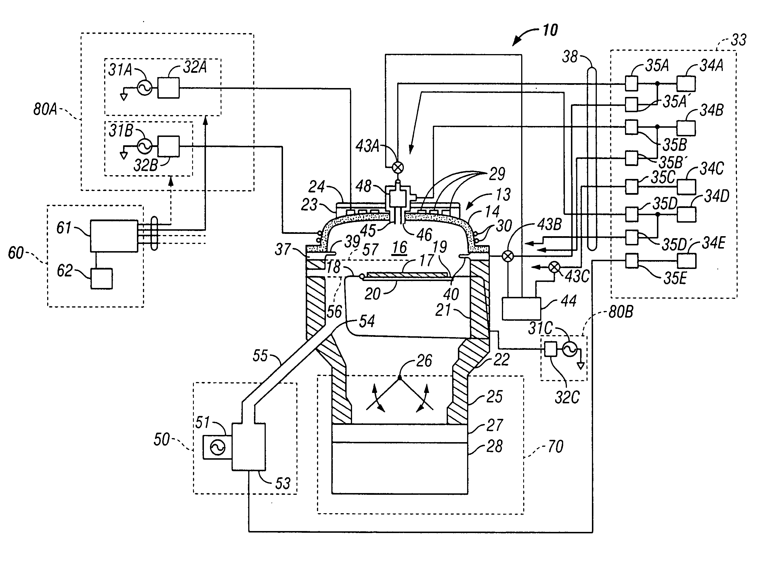
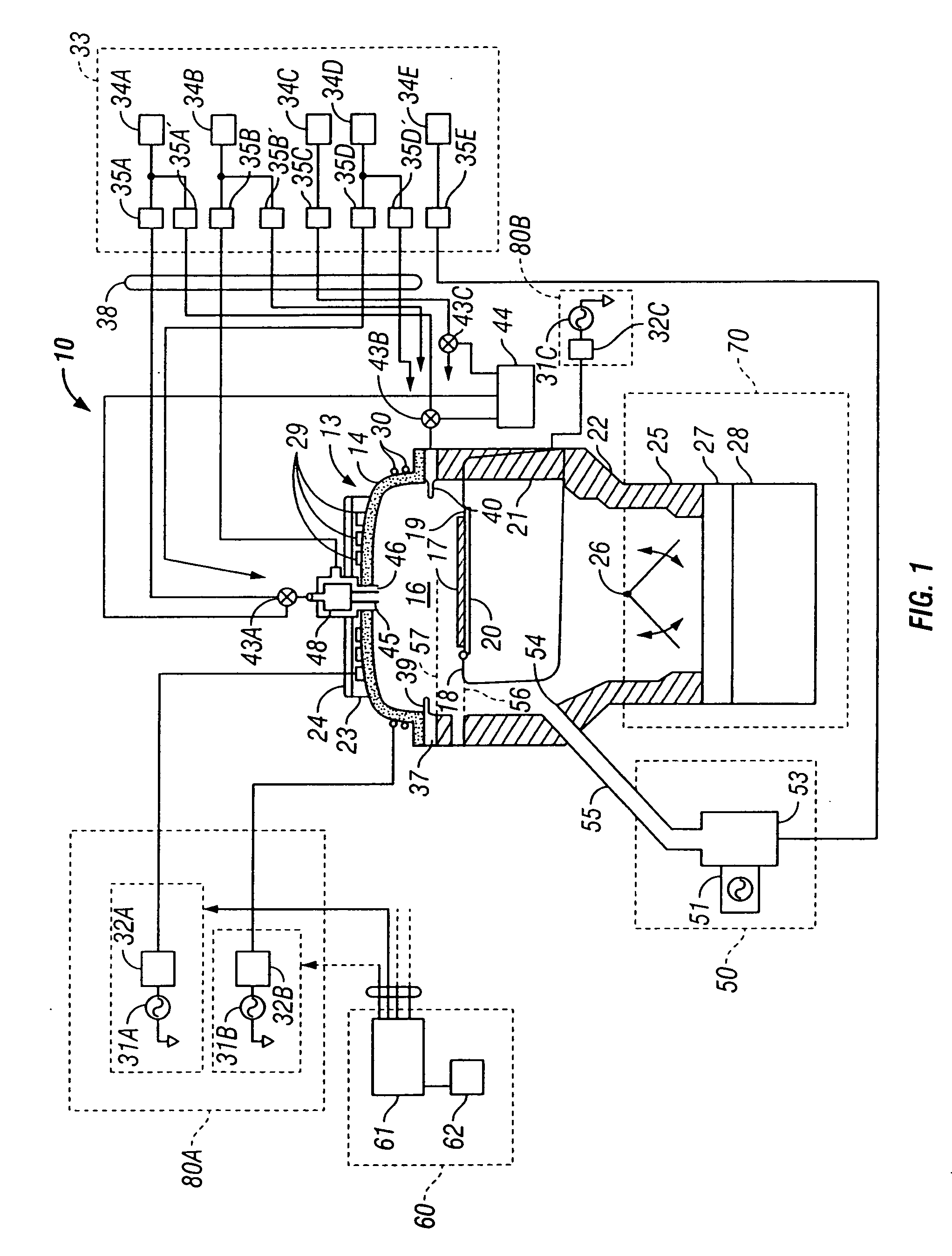
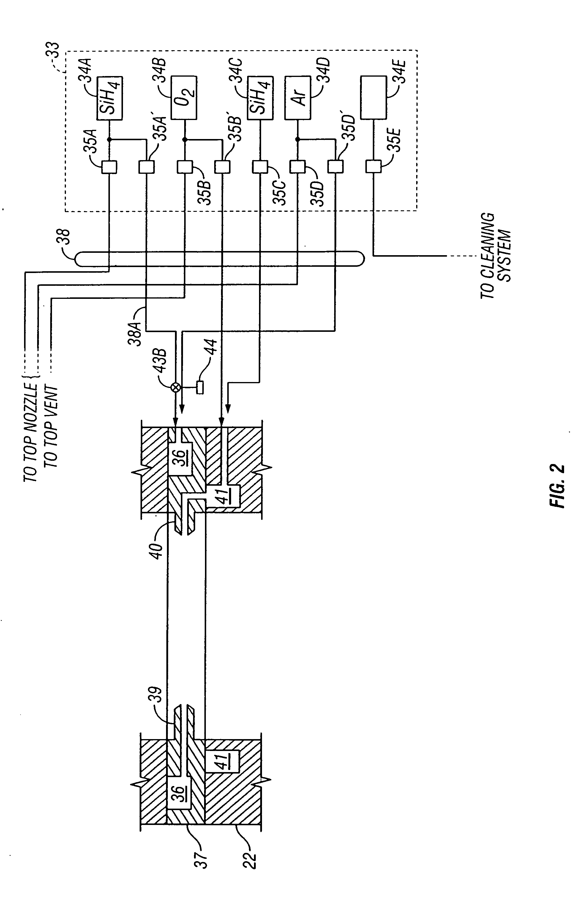
[0025]FIG. 1 illustrates one embodiment of a high density plasma chemical vapor deposition (HDP-CVD) system 10 in which a dielectric layer can be deposited. System 10 includes a chamber 13, a vacuum system 70, a source plasma system 80A, a bias plasma system 80B, a gas delivery system 33, and a remote plasma cleaning system 50.

[0026] The upper portion of chamber 13 includes a dome 14, which is made of a ceramic dielectric material, such as aluminum oxide or aluminum nitride. Dome 14 defines an upper boundary of a plasma processing region 16. Plasma processing region 16 is bounded on the bottom by the upper surface of a substrate 17 and a substrate support 18.

[0027] A heater plate 23 and a cold plate 24 surmount, and are thermally coupled to, dome 14. Heater plate 23 and cold plate 24 allow control of the dome temperature to within about ±10° C. over a range of about 100° C. to 200° C. This allows optimizing the dome temperature for the various processes. For example, it may be des...


PUM

PropertyMeasurementUnit
sizesaaaaaaaaaa
temperatureaaaaaaaaaa

Abstract

The present invention is directed to the design of a plasma CVD chamber which provides more uniform conditions for forming thin CVD films on a substrate. In one embodiment, an apparatus for processing semiconductor substrates comprises a chamber defining a plasma processing region therein. The chamber includes a bottom, a side wall, and a dome disposed on top of the side wall. The dome has a dome top and having a side portion defining a chamber diameter. A top RF coil is disposed above the dome top. A side RF coil is disposed adjacent the side portion of the dome. The side RF coil is spaced from the top RF coil by a coil separation. A ratio of the coil separation to the chamber diameter is typically at least about 0.15, more desirably about 0.2-0.25.

Description

CROSS-REFERENCES TO RELATED APPLICATIONS [0001] This application is a continuation of U.S. patent application Ser. No. 10 / 150,581, filed on May 17, 2002 which is herein incorporated by reference for all purposes. [0002] This application is also related to commonly assigned U.S. patent application Ser. No. 10 / 150,458; filed May 17, 2002, entitled “UPPER CHAMBER FOR HIGH DENSITY PLASMA CVD,” the entire disclosure of which is incorporated herein by reference.BACKGROUND OF THE INVENTION [0003] This invention relates generally to semiconductor processing equipment and, more particularly, to a chemical vapor deposition chamber suitable for high density plasma processing. [0004] Chemical vapor deposition (CVD) is a gas reaction process used in the semiconductor industry to form thin layers or films of desired materials on a substrate. Some high density plasma (HDP) enhanced CVD processes use a reactive chemical gas along with physical ion generation through the use of an RF generated plasm...

Claims


Application Information

Patent Timeline
Patent Type & Authority Applications(United States)
IPC IPC(8): C23C16/00C23C16/44C23C16/507H01J37/32
CPCC23C16/4401C23C16/507H01J37/321H01J37/32522
Inventor GONDHALEKAR, SUDHIRCHO, TOM K.GUENTHER, ROLFTAKEHIRO, SHIGERUNOHIRA, MASAYOSHIISHIKAWA, TETSUYAMUKUTI, NDANKA O.
Owner APPLIED MATERIALS INC
Why Eureka
Try Eureka