Etching Apparatus and Process with Thickness and Uniformity Control

a technology of uniformity control and etching apparatus, applied in microstructural technology, microstructured devices, electric discharge tubes, etc., can solve the problems of inefficiency and slow lapping and polishing process, unsuitable for removing silicon in a controlled non-uniform manner, and inability to achieve uniform etching uniformity, reduce the non-uniformity of remaining film, and reduce the overall wafer or film thickness. uniformity

Inactive Publication Date: 2006-08-31
ZAJAC JOHN +1
View PDF27 Cites 309 Cited by
  • Summary
  • Abstract
  • Description
  • Claims
  • Application Information

AI Technical Summary

Benefits of technology

[0025] It is the ability to change the distribution of reactant gas flow and/or gas composition automatically, in accordance with the direction from a control system, quickly and without manual intervention, that permits automatic adjustments to produce a desired distribution of individual film properties or wafer etching rate. The ability to do this for each wafer in accordance with that wafer's non-uniformity in thickness or film thickness (as measured by thickness measurement means discussed above) or other properties permits this invention to make the wafer or film more uniform (or less uniform as desired) after the process than before. This invention is capable of performing such uniformity improvement for symmetrically or asymmetrically non-uniform wafers or films by symmetrical or non-symmetrical etching uniformity control. Such controlled distributed etching may also be exercised to compensate for the normal non-uniformity in the process rate of a system which might result when using uniform gas distribution.
[0026] In some embodiments of this invention this process is accomplished using measurements of substrate or film thickness to provide information used in controlling the etching or deposition rate. In this case, the

Problems solved by technology

For production wafers to meet the more exacting site flatness specification required in the future using lapping and polishing process is inefficient and slow.
This is expensive since the lapping and polishing process is not well suited to controlled non-uniform removal rates.
Wet chemical removal of the silicon is possible but is currently unsuitable for removing silicon in a controlled non-uniform manner so as to yield wafers of uniform thickness.
Further, the cost, safety, and environmental concerns, limit the usefulness of this approach.
However, typical plasma etch processes used for integrated circuit manufacturing are typically too slow to be used for efficiently etching several of microns of silicon.
Further, these processes usually utilize energetic ion impact to promote etching and such ion bombardment at energies at or above 50 eV can cause crystalline defects in the silicon.
Hence, the key issue of controlled non-uniformity remains unaddressed by any of the conventional etch processes.
Plasma or reactive ion etching methods have never been shown to be capable of tailoring the non-uniformity of their etch rate for individual wafers so as to etch faster where they are thicker thus reducing their thickness variations.
Commonly in such applications large amounts of silicon or other substra

Method used


Image

  • Etching Apparatus and Process with Thickness and Uniformity Control
  • Etching Apparatus and Process with Thickness and Uniformity Control
  • Etching Apparatus and Process with Thickness and Uniformity Control

Examples


Embodiment Construction

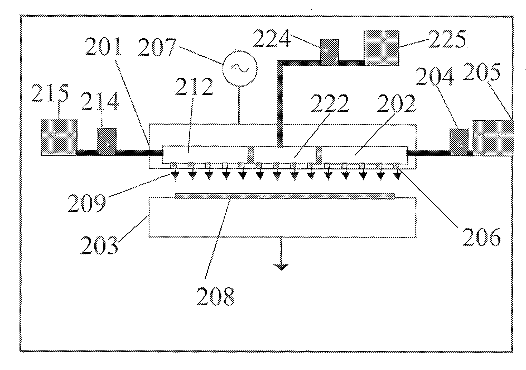
[0036] Etching of or thin film deposition on a substrate with a desired non-uniform rate or film properties are achieved in this invention by providing independent control of gas mixtures and / or gas flow rates to different parts of the processing plasma volume above the substrate.

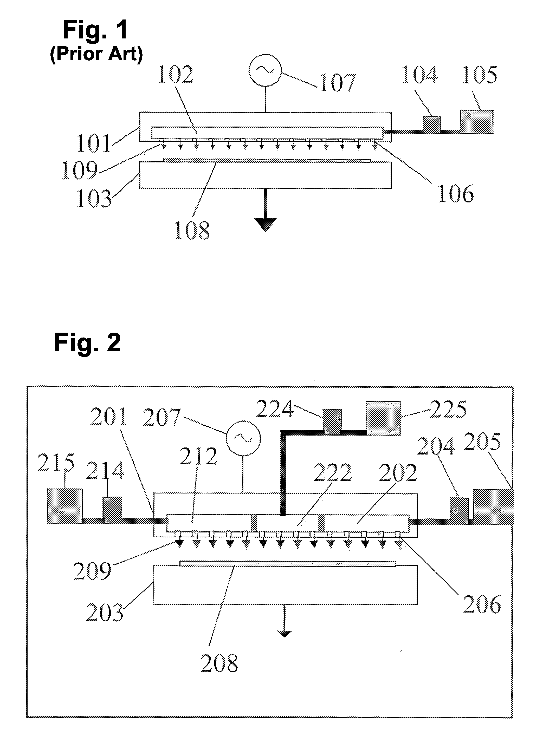
[0037] In one embodiment this may be accomplished using a showerhead (See FIG. 2) with a segmented gas reservoir. This figure illustrates a section view of a parallel plate embodiment of the reactor where the top, electrode is powered and where the wafer to be etched or deposited upon is placed on the bottom electrode. The radio frequency powered upper electrode 201, the cathode, is also used as a showerhead for the introduction of gases into the plasma discharge. Within said electrode are gas reservoirs 202, 212, 222 for distribution of the gas to the holes in certain areas of the structure. The lower electrode 203 is grounded electrically and serves therefore as the anode of the discharge. The gas supply...


PUM

PropertyMeasurementUnit
Fractionaaaaaaaaaa
Fractionaaaaaaaaaa
Thicknessaaaaaaaaaa

Abstract

Apparatus and process for etching semiconductor wafers and the like in which a substrate is supported by a pedestal within a chamber, and at least one gas capable of etching the substrate or a film material on the substrate is introduced into the chamber through a segmented gas injection element which is separated from the substrate by a distance approximately less than its size from which the distribution of the flow or mixture of gas can be altered spatially proximate to the substrate in a controlled and variable way, for each wafer or substrate if desired, by having a varying amount or mixture of gas flow to some or all of the segments such as to cause the etching rate distribution to vary across the substrate.

Description

CROSS REFERENCE TO RELATED APPLICATIONS [0001] This is a division of Ser. No. 09 / 886,580, filed Jun. 21, 2001.BACKGROUND OF THE INVENTION [0002] 1. Field of Invention [0003] This invention pertains generally to the processing of silicon wafers, other substrates, or other flat workpieces used in semiconductor, Micro-Electro-Mechanical Systems (MEMS), magnetoelectronic or flat panel display manufacturing and, more particularly, to the etching of, or deposition on such wafers, substrates or other workpieces. It provides an apparatus and method for rapidly changing in an automatic, controlled manner the spatial distribution of etching the workpiece or a film thereupon, or changing properties such as thickness or material properties of a film deposited across that substrate or workpiece. [0004] 2. Related Art [0005] One particular use of this invention may be as a part of the sequence of manufacturing steps for producing monocrystalline silicon wafers for semiconductor integrated circuit...

Claims


Application Information

Patent Timeline
IPC IPC(8): C03C25/68C23F1/00
CPCB81C1/00547H01J37/3244H01J37/32449
Inventor ZAJAC, JOHNSAVAS, STEPHEN EDWARD
Owner ZAJAC JOHN
Why Eureka
Try Eureka