Semiconductor device and method of manufacturing the same

a technology of semiconductor devices and semiconductors, applied in the direction of semiconductor devices, basic electric elements, electrical equipment, etc., can solve the problems of increased leakage current and reduced thickness of gate insulation films, and achieve the effects of reducing the reactivity of the gate electrode with the underlying gate insulation films, reducing leakage current, and reducing leakage curren

Active Publication Date: 2006-09-07
SONY CORP
View PDF1 Cites 5 Cited by
  • Summary
  • Abstract
  • Description
  • Claims
  • Application Information

AI Technical Summary

Benefits of technology

[0013] In the method of manufacturing a semiconductor device according to the another embodiment of the present invention, at least the gate insulation film side of the gate electrode is formed from the film containing hafnium and silicon in the step of forming the gate electrode, so that a compound of hafnium and silicon is formed at least at the interface between the gate electrode and the gate insulation film. Therefore, even when a silicon oxide film or a film containing silicon oxide as a main constituent is used as the gate insulation film, hafnium is restrained from undergoing a reduction reaction with the gate insulation film. Besides, the gate electrode can be so formed as to have a work function close to the work function of the conventional poly-Si gate electrode.
[0014] In the semiconductor device according to the one embodiment of the present invention, a compound of hafnium and silicon is formed at least at the interface between the gate electrode and the gate insulation film, so that the reactivity of the gate electrode with

Problems solved by technology

Thus, there has been the problem that, while the metallic material having work functions in the vicinity of 4.0 eV are suitable for obtaining a threshold value suited to NMOSFET and such metals include hafnium (Hf), zirconium (Zr) and t

Method used


Image

  • Semiconductor device and method of manufacturing the same
  • Semiconductor device and method of manufacturing the same
  • Semiconductor device and method of manufacturing the same

Examples


Embodiment Construction

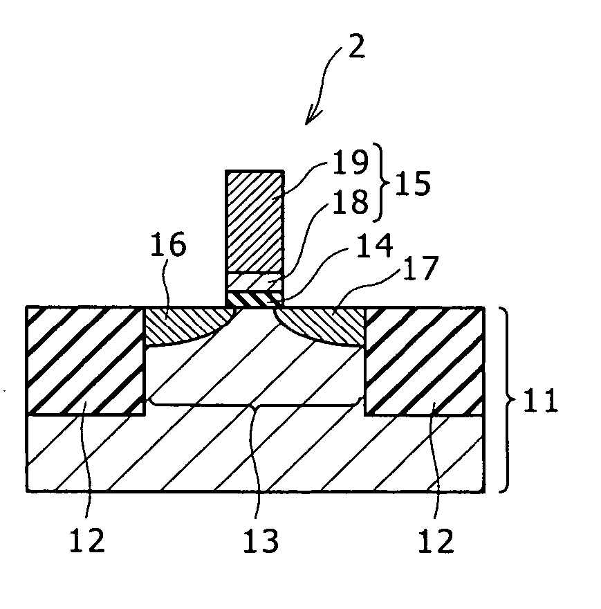
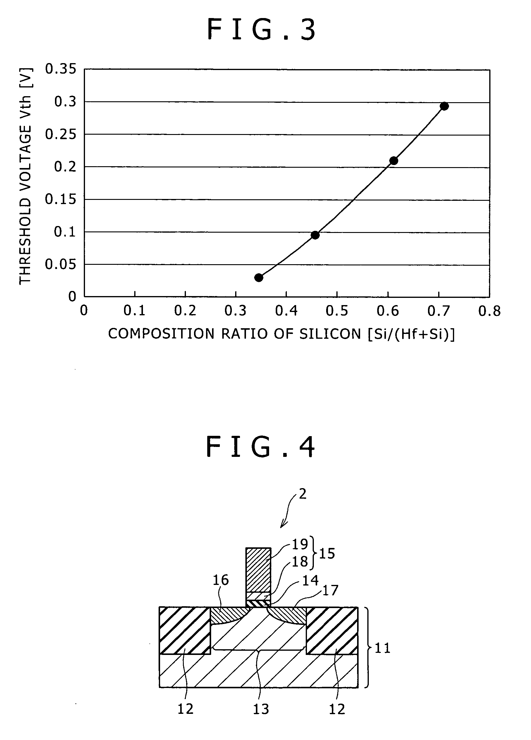
[0025] The semiconductor device according to the present invention is, for example, an NMOSFET having a gate electrode on a gate insulation film, wherein at least the gate insulation film side of the gate electrode is composed of a film containing silicon (Si) and hafnium (Hf), and the composition ratio Si / (Hf+Si) of silicon based on the total of hafnium and silicon is in the range of from 20 to 70%.

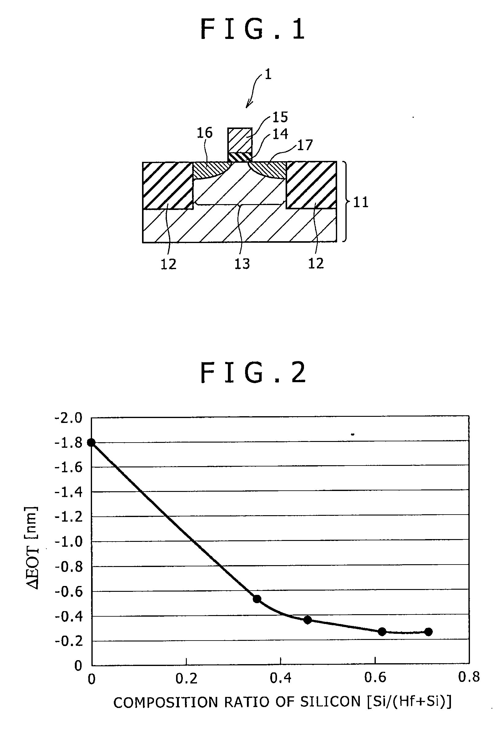
[0026] Now, a first example of an embodiment of the semiconductor device according to the present invention will be described below referring to the schematic configuration sectional diagram shown in FIG. 1. In FIG. 1, an NMOSFET will be described, as an example.

[0027] As shown in FIG. 1, device isolation regions 12 are formed in a semiconductor substrate 11, whereby a device forming region 13 is partitioned. A silicon substrate, as an example, is used as the semiconductor substrate 11, and the device isolation regions 12 are of an STI (Shallow Trench Isolation) structure, for example....


PUM


Abstract

A semiconductor device which includes a field effect transistor having a gate electrode on the upper side of a semiconductor substrate, with a gate insulation film therebetween, wherein at least the gate insulation film side of the gate electrode includes a film containing hafnium and silicon.

Description

CROSS REFERENCES TO RELATED APPLICATIONS [0001] The present invention contains subject matter related to Japanese Patent Application JP 2005-061999 filed in the Japanese Patent Office on Mar. 7, 2005, the entire contents of which being incorporated herein by reference.BACKGROUND OF THE INVENTION [0002] The present invention relates to a semiconductor device and a method of manufacturing the same such that the leakage current can be restrained and the gate insulation film can be made thinner. [0003] Enhancement of the degree of integration and the operating speed of transistors has been realized by miniaturizing the transistors based on the scaling rule. Thinning of the gate insulation film has progressed, and, for example, in transistors with a gate length of 0.1 μm or less, it may be necessary to reduce the thickness of the gate insulation film to or below 2 nm. Ordinarily, polycrystalline silicon (hereinafter referred to as poly-Si) has been used as a gate electrode material. The ...

Claims


Application Information

Patent Timeline
IPC IPC(8): H01L29/94H01L21/3205
CPCH01L21/28044H01L29/4916H01L29/78
Inventor YAMAGUCHI, SHINPEITAI, KAORIHIRANO, TOMOYUKI
Owner SONY CORP
Why Eureka
Try Eureka