Semiconductor device, stacked structure, and manufacturing method

a technology of semiconductor devices and stacked structures, applied in semiconductor devices, semiconductor/solid-state device details, electrical devices, etc., can solve the problems of insufficient heat dissipation mechanisms, device heat generation tendency overheating, and no heat dissipation path near the center of multi-chip devices, etc., to improve the heat dissipation properties of stacked multi-chip packages.

Active Publication Date: 2006-09-07
TAIWAN SEMICON MFG CO LTD
View PDF9 Cites 63 Cited by
  • Summary
  • Abstract
  • Description
  • Claims
  • Application Information

AI Technical Summary

Benefits of technology

[0008] An object of the present invention is to improve ...

Problems solved by technology

In this structure, the heat generated by the integrated circuit chips is to some extent dissipated to the ambient environment through the interconnecting plugs, but this heat dissipation mechanism is inadequate.
In particular, there is no path for dissipation of heat generated near the center of the multichip device.
The device therefore has a tendency to overheat, particularly in its central regions.
When the stacked structure forms a stacked multichip package, as the temperature...

Method used


Image

  • Semiconductor device, stacked structure, and manufacturing method
  • Semiconductor device, stacked structure, and manufacturing method
  • Semiconductor device, stacked structure, and manufacturing method

Examples


first embodiment

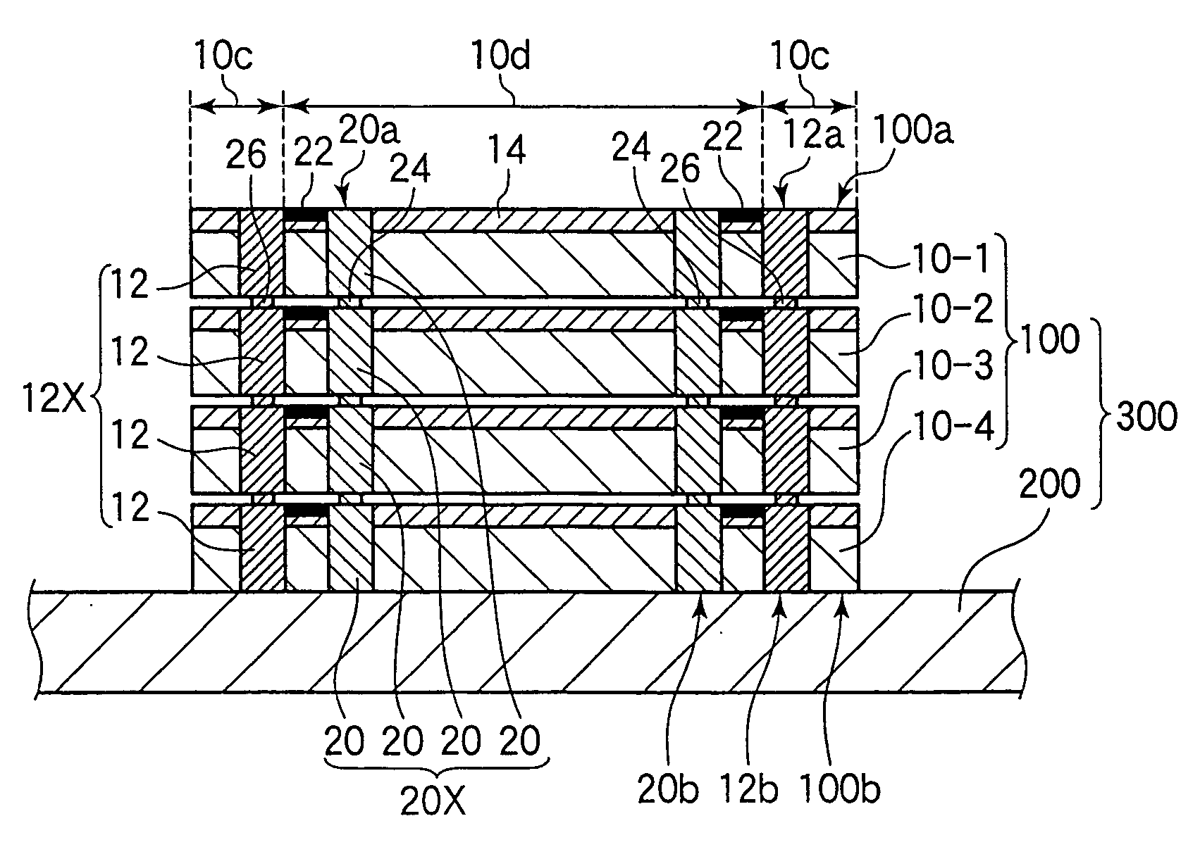
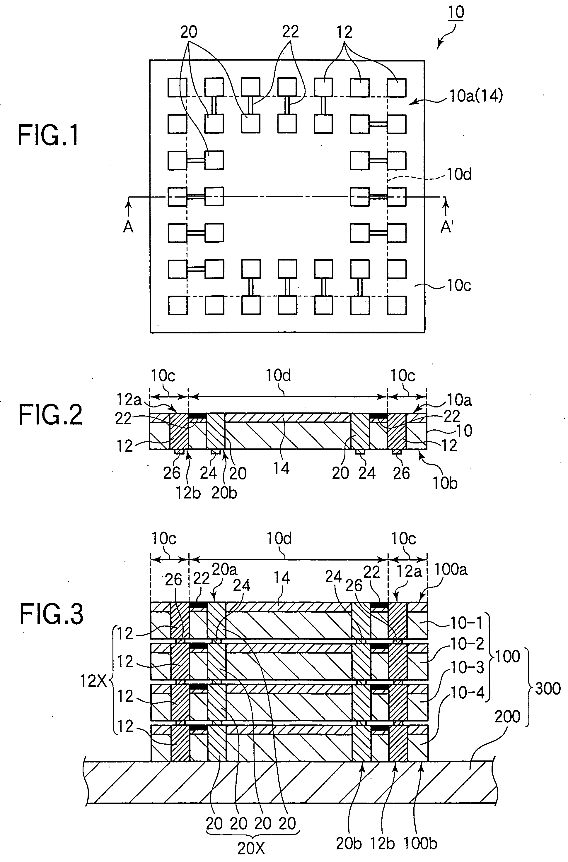
[0045] In the first embodiment, semiconductor devices of the type shown in FIGS. 1 and 2 are stacked as shown in FIG. 3. Each semiconductor device 10 has a silicon substrate covered by a dielectric protective film 14. The first major surface 10a of the device 10 is the outer surface of the dielectric protective film 14; the second major surface 10b of the device 10 is the undersurface of the silicon substrate.

[0046] Seen from the first and second major surfaces 10a and 10b, the semiconductor device 10 is rectangular in shape. The semiconductor device 10 accordingly has the form of a rectangular solid, although the first embodiment is not limited to this particular form.

[0047] The semiconductor device 10 has a plurality of electrically conductive members referred to below as electrical vias 12 that function as paths for input and output signals, or as power and ground paths, for microelectronic circuits formed below the dielectric protective film 14. The electrical vias 12 are disp...

second embodiment

[0082] A second embodiment of the present invention will be described with reference to FIGS. 19 and 20. The second embodiment adds a heat dissipator to the stacked and mounted structures described in the first embodiment. The heat dissipator is located on the top surface of the stacked structure to provide improved dissipation of heat generated by the semiconductor devices 10 to the ambient environment.

[0083] The heat dissipator 30 in the second embodiment is a silicon heat sink having an upper surface 30a and a lower surface 30b, with fins 30c extending from the upper surface 30a as shown in FIG. 20. The heat dissipator 30 rests atop the uppermost semiconductor device 10-1 in the stacked structure 100, so the top surface 100a of the stacked structure 100 is now the upper surface of the fins 30c. The lower surface 30b of the heat dissipator 30 is connected by thermal conduction bumps 28 to the electrically conductive columns 12X and thermally conductive columns 20X. Heat generated...

third embodiment

[0087] The third embodiment of the present invention adds a heat dissipating coating to the stacked and mounted structures of the second embodiment. Referring to FIGS. 21 and 22, the coating 40 covers all exposed surfaces of the mounted structure 300, including the upper surface 30a of the heat dissipator 30, the upper and side surfaces of the fins 30c, the sides of the individual semiconductor devices 10, and the surface of the mounting substrate 200.

[0088] The coating 40 comprises a material that promotes dissipation of heat generated by the mounted stacked structure, such as a known liquid ceramic paint that promotes thermal radiation and has a heat dissipation ratio of about 0.92.

[0089] The coating 40 is formed by spraying liquid ceramic paint, for example, onto the exposed areas of the mounted structure 300 after the semiconductor devices 10 are stacked and the stacked structure 100 is mounted on the mounting substrate 200.

[0090] The coating 40 can enhance the heat dissipati...


PUM


Abstract

An array of electrically conductive members, formed around the edges of a semiconductor device or chip, penetrate from one major surface of the device to the other major surface. In an area located inward of this array, a multiplicity of thermally conductive members also penetrate from one major surface to the other major surface. The semiconductor device can be manufactured from a semiconductor wafer by creating holes that penetrate partway through the wafer, filling the holes with metal to form the electrically conductive members and thermally conductive members, and then grinding the lower surface of the wafer to expose the ends of the electrically conductive members and thermally conductive members before dicing the wafer into chips. The thermally conductive members improve heat dissipation performance when semiconductor chips of this type are combined into a stacked multichip package.

Description

BACKGROUND OF THE INVENTION [0001] 1. Field of the Invention [0002] The present invention relates to a semiconductor device and its manufacturing method, to a stacked structure including the semiconductor device, and to a package including the stacked structure. [0003] 2. Description of the Related Art [0004] Multichip semiconductor devices in which a plurality of semiconductor chips are stacked in various ways are under development for the twin purposes of greater functionality and greater integration. One example is described in Japanese Patent Application Publication No. 10-223833, which discloses a semiconductor device comprising a stack of semiconductor integrated circuit chips interconnected by plugs and bumps. [0005] In this structure, the heat generated by the integrated circuit chips is to some extent dissipated to the ambient environment through the interconnecting plugs, but this heat dissipation mechanism is inadequate. In particular, there is no path for dissipation of ...

Claims


Application Information

Patent Timeline
IPC IPC(8): H01L29/00
CPCH01L23/3677H01L23/481H01L25/0657H01L2225/06513H01L2225/06541H01L2225/06589H01L2224/16H01L2224/0554H01L2224/05573H01L2224/05647H01L2224/06135H01L2224/13025H01L2924/00014H01L2224/05599H01L2224/0555H01L2224/0556
Inventor NOGUCHI, TAKASHI
Owner TAIWAN SEMICON MFG CO LTD
Why Eureka
Try Eureka