Electron beam writing system and electron beam writing method
a writing system and electron beam technology, applied in the field of electron beam writing system, can solve the problems of deflection distortion within the patterned electron beam formed by high-speed scanning that cannot be detected and corrected, and the size of the opening of the mark is degraded in this method, so as to achieve precise correction of deflection
- Summary
- Abstract
- Description
- Claims
- Application Information
AI Technical Summary
Benefits of technology
Problems solved by technology
Method used
Image

Examples
first embodiment
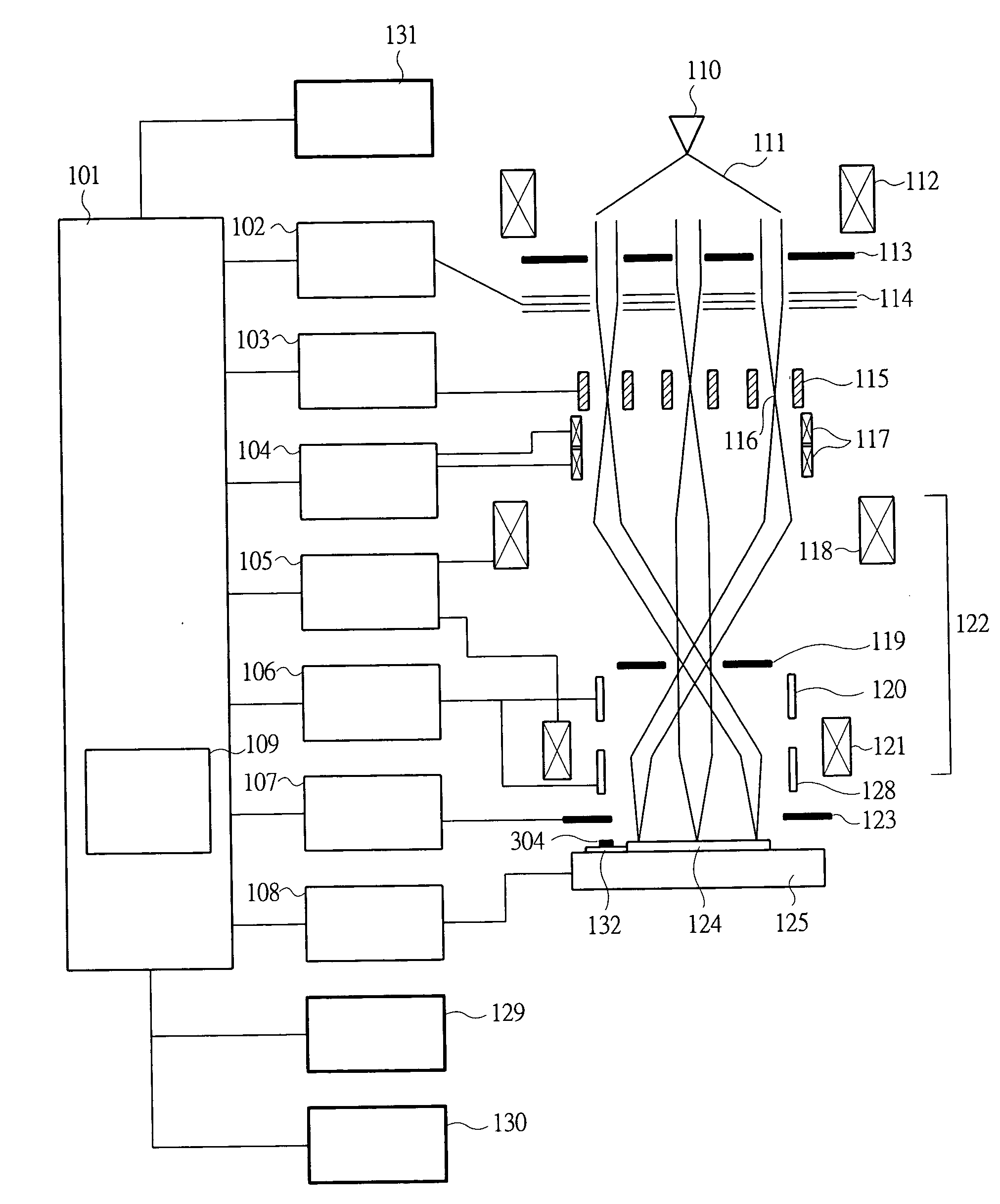
[0038]FIG. 1 is a diagram showing a configuration of an electron beam writing system according to an embodiment of the present invention, and FIG. 16 is a block diagram showing a detailed configuration of a central control unit in the electron beam writing system according to this embodiment.
[0039] First, an example of the configuration of the electron beam writing system according to this embodiment will be described with reference to FIG. 1 and FIG. 16. The electron beam writing system of this embodiment is comprised of: for example, an electron optical system including an electron gun 110, a condenser lens 112, an aperture array 113, a lens array 114, a blanker array 115, aligners 117, a first projector lens 118, a blanking aperture 119, a first deflector 120, a second projector lens 121, a second deflector 128, and others; a control system including a central control unit 101, a focus control circuit 102, a blanking circuit 103, an aligner control circuit 104, a lens control ci...
second embodiment
[0061] Next, the correction of deflection distortion will be described. Note that the configuration of the electron beam writing system according to a second embodiment of the present invention is same as that of the first embodiment which is shown in FIG. 1 and FIG. 16.
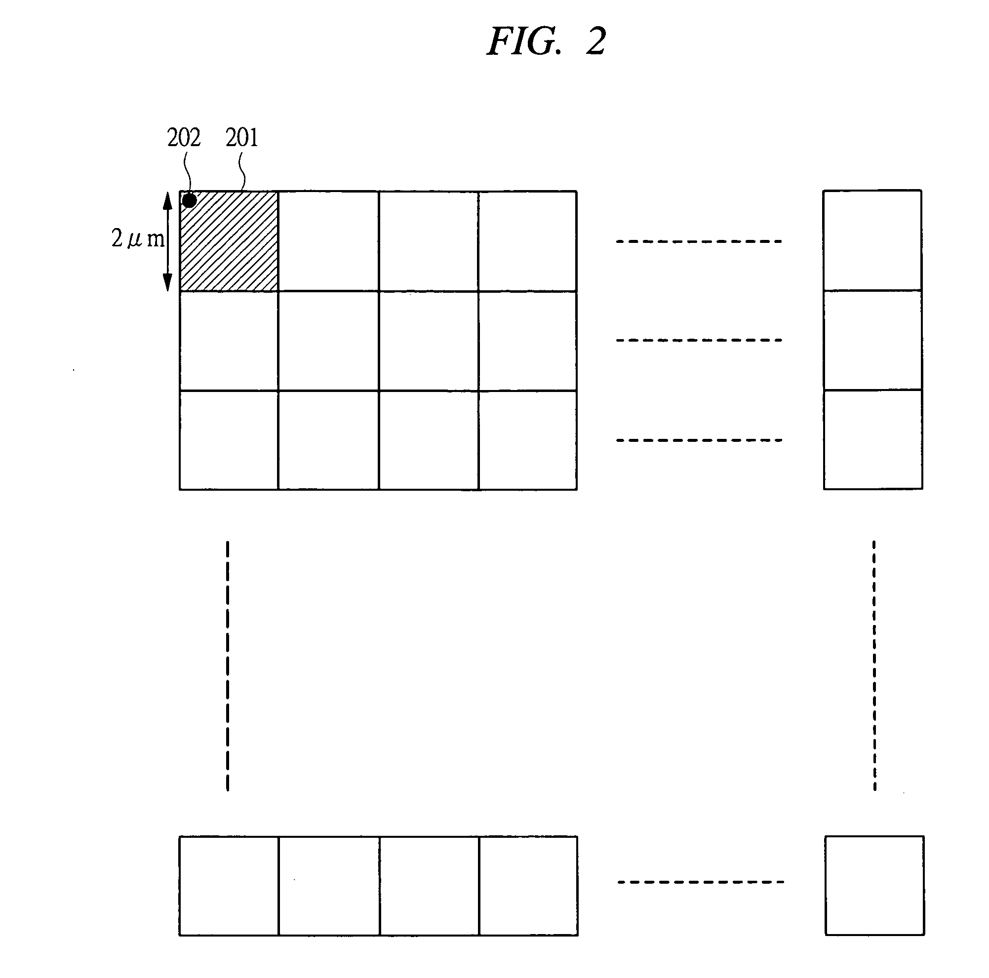
[0062] In conventional methods, since a distortion amount in a 2-μm-square electron beam cannot be measured, it is difficult to correct distortion of the pattern position of a 2 μm square in the actual writing.
[0063] On the other hand, correction is performed in the following manner in the present invention. First, deflection amount correction is performed in the same manner as that of the first embodiment by use of the correction marks 306 in which five rectangular openings each having a width of 0.2 μm and a height of 2 μm are arranged at a pitch of 0.4 μm and the beam obtained by performing the high-speed deflection scanning 301 so that five rectangular beams each having a width of 0.2 μm and a height of 2 μm ar...
third embodiment
[0066] In a third embodiment of the present invention, multi-beams comprised of a plurality of electron beams are used. Note that the configuration of the electron beam writing system according to the third embodiment is the same as that of the first embodiment shown in FIG. 1 and FIG. 16.
[0067]FIG. 11 is a diagram showing a scanning method according to the third embodiment. In FIG. 11, the central control unit 101 performs the high-speed deflection scanning 301 on the entire surface of the minute fields 201 so that adjacent multi-beams form five rectangular patterned electron beams 305 each having a width of 0.2 μm and a height of 2 μm, which are arranged at a pitch of 0.4 μm. Consequently, as shown in FIG. 11, the patterned electron beams 305 of about 2 μm×4 μm are formed in one cycle of the high-speed deflection scanning. The patterned electron beams 305 are used to perform the low-speed deflection scanning 303 on the correction marks 306 in which five rectangular opening correc...
PUM
 Abstract
Description
Claims
Application Information
 - Generate Ideas
- Intellectual Property
- Life Sciences
- Materials
- Tech Scout
- Unparalleled Data Quality
- Higher Quality Content
- 60% Fewer Hallucinations
Browse by: Latest US Patents, China's latest patents, Technical Efficacy Thesaurus, Application Domain, Technology Topic, Popular Technical Reports.
© 2025 PatSnap. All rights reserved.Legal|Privacy policy|Modern Slavery Act Transparency Statement|Sitemap|About US| Contact US: help@patsnap.com