Delay locked loop for controlling duty rate of clock

a technology of duty rate and delay lock, which is applied in the direction of pulse generator, pulse manipulation, pulse technique, etc., can solve the problems of high cost, time-consuming and labor-intensive, and delay time between the external clock and the internal clock

Active Publication Date: 2006-09-07
SK HYNIX INC
View PDF65 Cites 44 Cited by
  • Summary
  • Abstract
  • Description
  • Claims
  • Application Information

AI Technical Summary

Benefits of technology

[0015] It is, therefore, an object of the present invention to provide a delay locked loop (DLL) capable of controlling a duty rate of a clock by a fuse option or an extended mode register set (EMRS) input, without any modification of a mask.

Problems solved by technology

When an external clock is used for an internal circuit, there is inevitably generated a delay time between the external clock and an internal clock.
Meanwhile, it is difficult for the first and the second DLL clocks RCLK_DLL and FCLK_DLL generated through the aforementioned process, to have a duty rate of about 50% due to various factors such as a manufacturing process, a driving voltage level, a temperature variance, and so forth.
Also, in order to adjust the duty rate after the fabrication of a chip, there has been only a method for re-modifying a mask in the prior art so that high expense and much time are needed after all.

Method used


Image

  • Delay locked loop for controlling duty rate of clock
  • Delay locked loop for controlling duty rate of clock
  • Delay locked loop for controlling duty rate of clock

Examples


first embodiment

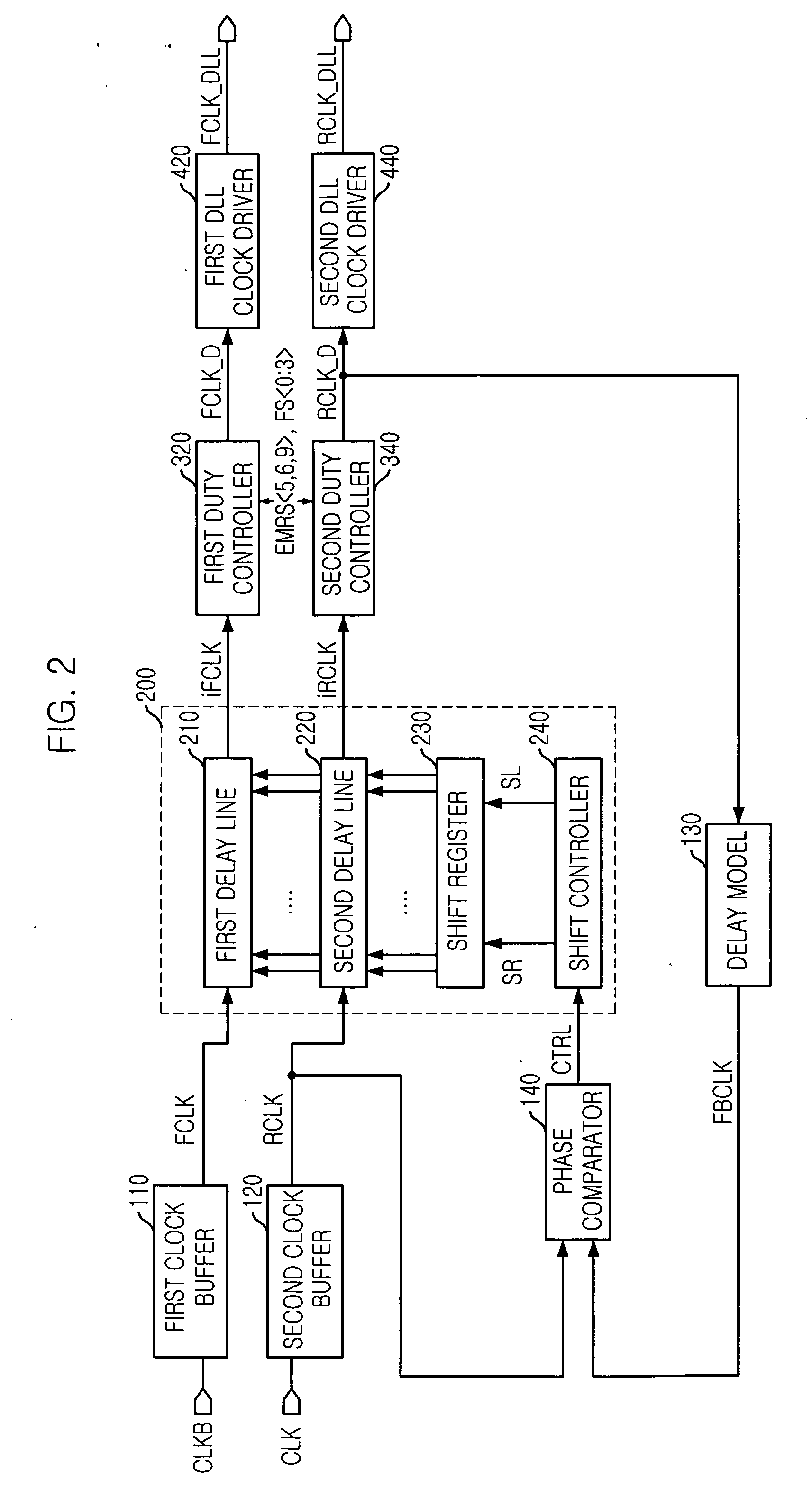
[0026]FIG. 2 is a block diagram setting forth a register-controlled DLL in accordance with the present invention.

[0027] Referring to FIG. 2, the DLL of the present invention includes a first clock buffer 110, a second clock buffer 120, a first delay line 210, a second delay line 220, a shift register 230, a first duty controller 320, a second duty controller 340, a first DLL driver 420, a second DLL driver 440, a delay model 130, a phase comparator 140, and a shift controller 240.

[0028] Herein, the first clock buffer 110 receives an external clock bar signal CLKB and generates an internal falling clock FCLK in synchronization with a falling edge of an external clock signal CLK. The second clock buffer 120 receives the external clock signal CLK and generates an internal rising clock signal RCLK in synchronization with a rising edge of the external clock signal CLK.

[0029] The first delay line 210 receives the internal falling clock FCLK in synchronization with the falling edge of th...

second embodiment

[0048]FIG. 5 is a block diagram setting forth a DLL in accordance with the present invention.

[0049] Referring to FIG. 5, it is understood that the DLL of the second embodiment does not employ a clock buffer, a delay line and a duty controller for an external clock bar signal CLKB because the external clock bar signal CLKB is not applied to the DLL, which is different from the DLL of FIG. 2. The reason is that the DLL of the second embodiment includes a clock buffer 120 of a CMOS inverter type.

[0050] Therefore, in accordance with the second embodiment of the present invention, a duty controller 360 receives an output clock iRCLK of a delay line 220 so as to generate a falling DLL clock FCLK_D and a rising DLL clock RCLK_D for controlling a duty rate.

[0051]FIG. 6 is a circuit diagram illustrating the duty controller 360 of FIG. 5.

[0052] Referring to FIG. 6, a signal generator 368 of the duty controller 360 is provided with a latch unit 368a, a buffer 368b for outputting the rising ...


PUM


Abstract

There is provided a DLL capable of controlling a duty rate of a clock by a fuse option or an EMRS input. The DLL includes a first clock buffer, a second clock buffer, a first delay line, a second delay line, a shift register, a first duty control unit, a second duty control unit, a first DLL driver, a second DLL driver, a delay model, a phase comparator, and a shift control unit. In the DLL, a first duty control unit and a second duty control unit control each duty rate of the output clocks of a first and a second delay lines respectively through the EMRS input or the fuse option. Therefore, it is possible to control the duty rate of DLL clocks through the EMRS input or the fuse option.

Description

FIELD OF THE INVENTION [0001] The present invention relates to a design technology for a semiconductor device; and more particularly, to a delay locked loop (DLL) for controlling a duty rate of a clock. DESCRIPTION OF RELATED ART [0002] Typically, a clock is used as a reference for adjusting an operational timing in a system or circuit of a semiconductor memory device. In particular, the clock is also used for securing high-speed and error-free operation in the system or the circuit. When an external clock is used for an internal circuit, there is inevitably generated a delay time between the external clock and an internal clock. This is so called a clock skew. Therefore, in order to compensate the delay time and to equalize a phase of the internal clock with that of the external clock, a delay locked loop (hereinafter, referred to as a DLL) is typically used in the semiconductor memory device. [0003] In addition, the DLL are broadly used in a synchronous semiconductor memory device...

Claims


Application Information

Patent Timeline
Patent Type & Authority Applications(United States)
IPC IPC(8): H03L7/06
CPCH03L7/0805H03L7/0814H03L7/0816B66F9/165B66F17/003
Inventor KANG, YONG-GU
Owner SK HYNIX INC
Why Eureka
Try Eureka