Protection of output stage transistor of an RF power amplifier

Active Publication Date: 2006-09-07
STMICROELECTRONICS SRL
View PDF7 Cites 21 Cited by
  • Summary
  • Abstract
  • Description
  • Claims
  • Application Information

AI Technical Summary

Benefits of technology

[0018] According to one aspect of the protection circuit, the reference threshold voltage is set by an externally applied regulating voltage and by processing it to compensate for possible in

Problems solved by technology

Modern cellular radio mobile communication systems may impose power efficiency and ruggedness specifications that cause exceptional technical problems to the designers of the RF transmission circuits.
A typical example of these systems is GSM, where the mobile equipment is not allowed a permanent failure even under a severe load impedance mismatch.
First, no voltage regulator is used between the battery cells and the power amplifier.
A higher than 2 watt output power level is required for GSM power amplifiers, which implies a strong current consumption.
In such conditions, the use of a linear voltage regulator would result in excessive power losses due to large voltage drops, unless an application-specific regulator was properly tailored to the equipment.
As far as efficiency is concerned, switching-mode voltage regulators offer better performance than linear ones, but the output power spectrum may be seriously compromised by spurious tones resulting from a residual ripple on the supply voltage.
The drawback with this approach is that an oversupply condition occurs each time the mobile handset is put in the battery-charge state.
As a result, the PA can incur strong load mismatch conditions due to antenna faults or disconnection.
The worst-case conditions occur when the power amplifier is subject both to oversupply and load mismatch.
The ability of silicon bipolar devices to operate with collector peaks beyond the nominal (dc) breakdown voltage has been demonstrated, whereas GaAs HBTs cannot survive such a test.
Despite this, too high breakdown voltages (i.e., more than thr

Method used


Image

  • Protection of output stage transistor of an RF power amplifier
  • Protection of output stage transistor of an RF power amplifier
  • Protection of output stage transistor of an RF power amplifier

Examples


Embodiment Construction

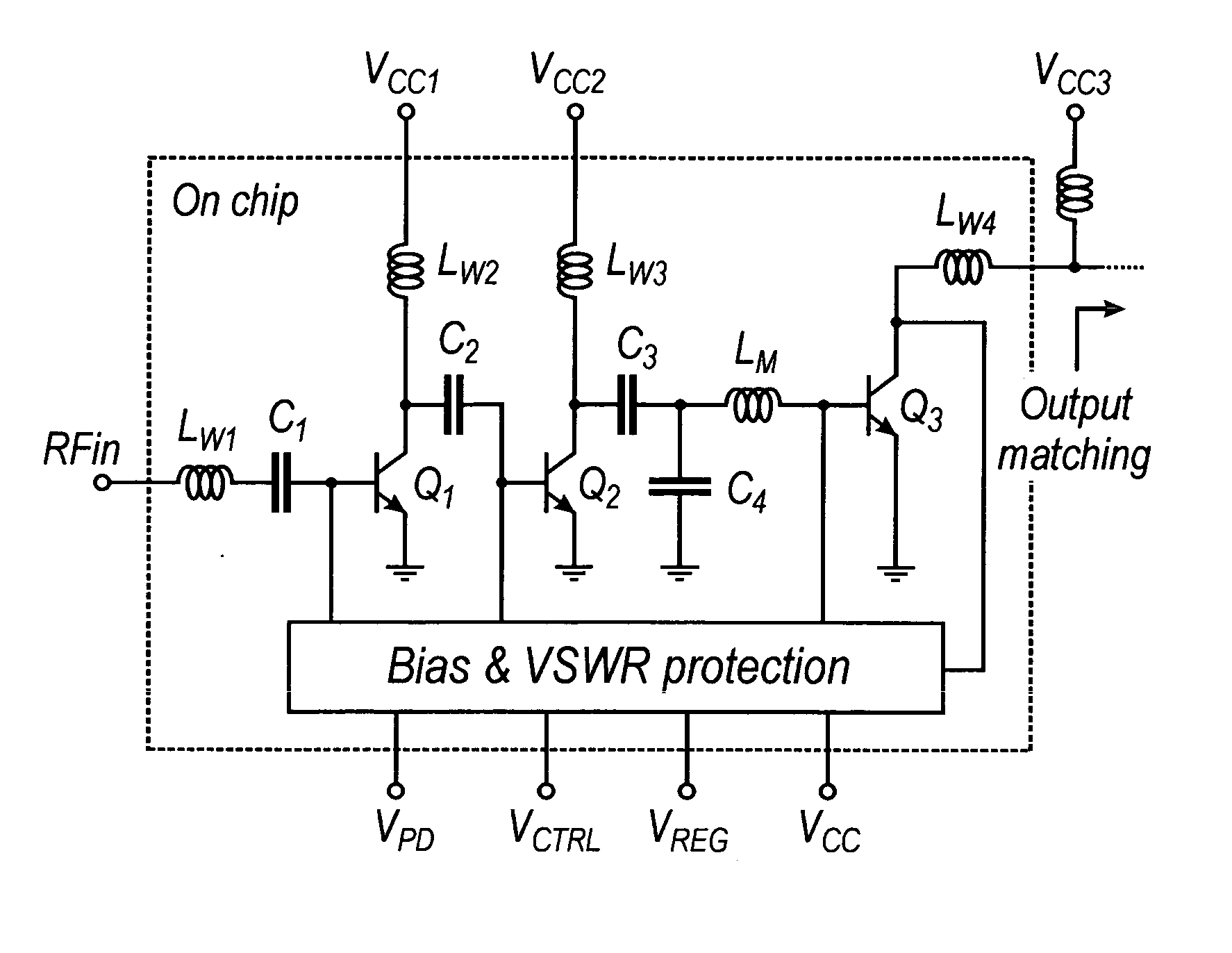
[0036] A simplified diagram of an RF power amplifier (briefly PA) according to a sample embodiment is shown in FIG. 7. The circuit includes three stages (Q1-Q3) Based on load-pull measurements, two elementary power cells were paralleled to implement the first stage, seven cells were used for the-second stage, and twenty-eight cells for the third.

[0037] In GSM and DCS systems, transmitter linearity requirements are a minor issue due to the constant-envelope modulation scheme adopted. Therefore, high-efficiency operation classes, such as disclosed in F. H. Raab, “Class-F power amplifiers with maximally flat waveforms,”IEEE Trans. Microwave Theory Tech., vol. 45, pp. 2007-2012, Nov. 1997, can be exploited for PA design. In the embodiment considered, a series-resonant load was used to improve PA efficiency as disclosed in F. Carrara, T. Biondi, A. Castorina, A. Scuderi, and G. Palmisano, “A 1.8-GHz high-efficiency 34-dBm silicon bipolar power amplifier,”IEEE Trans Microwave. Indeed, bo...


PUM


Abstract

A protection method may prevent a load-mismatch-induced failure in solid-state power amplifiers. In an RF power amplifier, the load voltage standing-wave ratio results in very high voltage peaks at the collector of the final stage and may eventually lead to permanent failure of the power transistor due to avalanche breakdown. The method avoids breakdown by attenuating the input power to the final stage during overvoltage conditions, thus limiting the output collector swing. This is accomplished by a feedback control system, which detects the peak voltage at the output collector node and clamps its value to a given threshold by varying the circuit gain. Indeed, the control loop is unlocked in the nominal condition and it acts when an output mismatching condition is detected. A control circuit also allows a supply-independent collector-clamping threshold to be accurately set.

Description

FIELD OF THE INVENTION [0001] The present invention relates to the field of electronics, and, more particularly, to radio frequency (RF) power amplifiers and associated methods. BACKGROUND OF THE INVENTION [0002] Modern cellular radio mobile communication systems may impose power efficiency and ruggedness specifications that cause exceptional technical problems to the designers of the RF transmission circuits. A typical example of these systems is GSM, where the mobile equipment is not allowed a permanent failure even under a severe load impedance mismatch. In most commercial GSM mobile equipment, worst-case mismatch conditions are determined by two customary system features. [0003] First, no voltage regulator is used between the battery cells and the power amplifier. A higher than 2 watt output power level is required for GSM power amplifiers, which implies a strong current consumption. In such conditions, the use of a linear voltage regulator would result in excessive power losses...

Claims


Application Information

Patent Timeline
IPC IPC(8): H03G3/20
CPCH03F1/52H03F3/19H03F2200/447H03F2200/78H04B1/0466
Inventor SCUDERI, ANGELOSCUDERI, ANTONINOLA PAGLIA, LUCACARRARA, FRANCESCOPALMISANO, GIUSEPPE
Owner STMICROELECTRONICS SRL
Why Eureka
Try Eureka