

Light transmission and reception module, sub-mount, and method of manufacturing the sub-mount
- Summary
- Abstract
- Description
- Claims
- Application Information
AI Technical Summary
Benefits of technology
Problems solved by technology
Method used
Image

Examples
first embodiment
[0063] With referring to the drawings, a first embodiment of the present invention is specifically described below.
[Light Transmission and Reception Module]
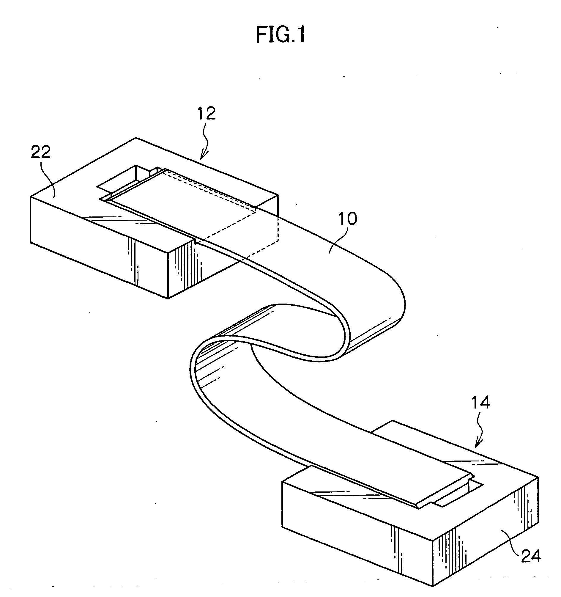
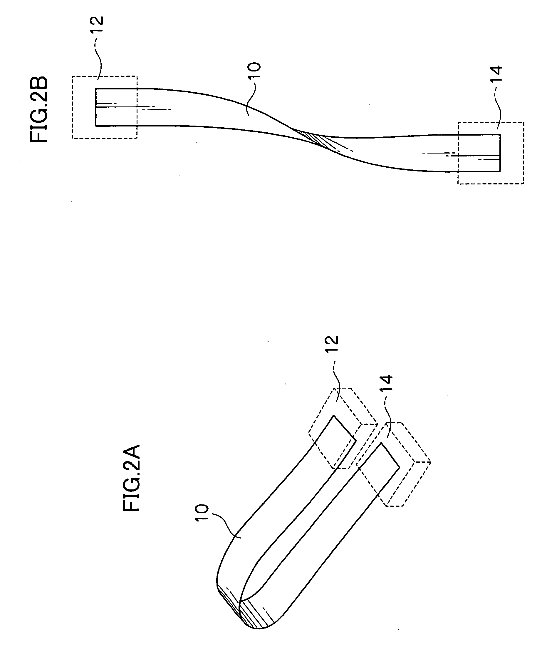
[0064]FIG. 1 is a schematic structural diagram of light transmission and reception module in the first embodiment. This light transmission and reception module is composed of, as shown in FIG. 1, a belt-shaped macromolecular optical waveguide film 10, and optical transmission and reception sections 12, 14 for transmitting and receiving an optical signal through an optical waveguide formed in the macromolecular optical waveguide film 10.
[0065] The optical transmitter 12 has a sub-mount 22, and one end of the macromolecular optical waveguide film 10 is held on the sub-mount. The optical transmission and reception section 14 has a sub-mount 24, and other end of the macromolecular optical waveguide film 10 is held on the sub-mount 24.
[0066] The macromolecular optical waveguide film 10 is composed of a flexible transparent resin f...
second embodiment
[0181] Referring now to the drawings, a second embodiment of the invention is specifically described below.
[Light Transmission and Reception Module]
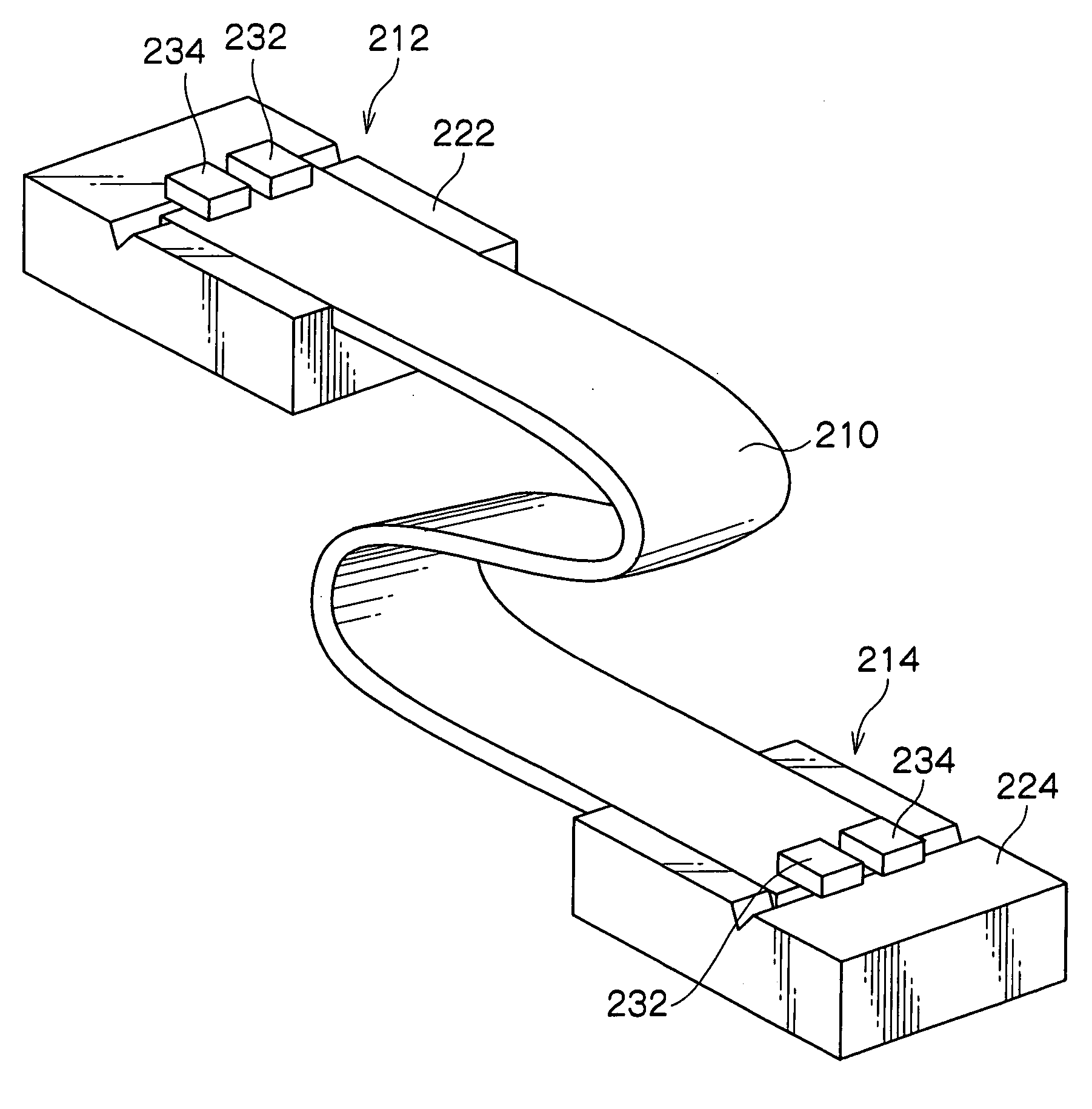
[0182]FIG. 9 is a schematic structural diagram of light transmission and reception module in the second embodiment. This light transmission and reception module is composed of, as shown in FIG. 9, a belt-shaped macromolecular optical waveguide film 210, and optical transmission and reception sections 212, 214 for transmitting and receiving an optical signal through an optical waveguide formed in the macromolecular optical waveguide film 210. The optical transmitter 212 has a surface emission type semiconductor laser diode (LD) 232 as light emitting element, a photo diode (PD) 234 as light detecting element, and a sub-mount 222, and one end of the macromolecular optical waveguide film 210 is held on the sub-mount 222. The optical transmission and reception section 214 has LD 232, PD 234, and sub-mount 224, and other end of the macromole...
third embodiment
[0239] Referring now to the drawings, a third embodiment of the invention is specifically described below.
[Manufacturing Method of Sub-Mount]
[0240] A method of manufacturing a sub-mount of the invention comprises (1) a mold production step of producing a mold having projections and recesses for copying the surface configuration of a sub-mount, (2) a filling step of filling the produced mold with curing material, (3) a curing step of curing the applied curing material, and (4) a releasing step of separating a copied sub-mount from the mold.
[0241] A method of producing a mold includes (A) a method of producing a mold by curing liquid silicone rubber on master plate of sub-mount, (B) a method of producing a mold by etching a silicon substrate, and (C) a method of producing a mold by casting a metal. The manufacturing method of the sub-mount using the mold produced in method (A) will be referred to as “the duplication method using silicone resin” hereinafter, and the manufacturing me...
PUM
 Abstract
Description
Claims
Application Information