
Microimprint/nanoimprint device

Inactive Publication Date: 2006-09-07
IND TECH RES INST
View PDF6 Cites 23 Cited by
  • Summary
  • Abstract
  • Description
  • Claims
  • Application Information

AI Technical Summary

Benefits of technology

[0013] In light of the drawbacks in the foregoing conventional technology, an objective of the present invention is to provide a microimprint / nanoimprint device, which provides a function of performing different imprinting processes and simplifies the structure thereof.
[0014] Another objective of the present invention is to provide a microimprint / nanoimprint device, which can complete large area imprinting at a time and thus increases the production yields.
[0015] Still another objective of the present invention is to provide a microimprint / nanoimprint device, which can perform uniform imprinting and thus improves the molding quality.

Problems solved by technology

However, as the line width and line pitch processed for various kinds of products are continuously decreased to smaller than 100 nanometers, the current photo-lithography technology encounters a physical problem in optical imaging, and the fabrication difficulty and costs of fabrication equipment are also greatly increased.
Although a next-generation lithography technology has been proposed, it still has problems of high equipment costs and low yields.
This not only complicates the design of ultraviolet source but also greatly increases the device costs.
Further, the microimprint / nanoimprint device may only be applied to a small area imprinting process.
Consequently, this conventional technology prolongs a product fabrication period of time and may affect the product yields directly due to errors of alignment precision between the periods.
However, when employing the fluid pressure imprint lithography device disclosed in U.S. Pat. No. 6,482,742, it must spend time on changing system modules, thereby increasing the device costs.
This increases processing costs before and after imprinting, and makes control of the fabrication processes not continuous, thereby prolonging a molding period and not favorable for mass production.
Moreover, the sealing envelope generally has relatively poorer light penetrability, such that when ultraviolet needs to go through the light penetrable window and the sealing envelope, the ultraviolet energy is apt to be absorbed during transmission or even becomes scattered.
As this conventional technology cannot control the provided ultraviolet energy and cannot obtain a uniformly imprinted product, the molding quality of the molding material would be affected.
Therefore, it is greatly desirable to develop a microimprint / nanoimprint device, capable of solving the problems in the foregoing conventional technology such as high costs, low yields, poor quality and unfavorable for mass production, which are caused by the drawbacks such as having a complicated design of light source mechanism, high equipment costs, small imprinting area, increased processing costs, discontinuous control of fabrication processes, a prolonged molding period, and difficulty in controlling the molding quality.

Method used


Image

  • Microimprint/nanoimprint device
  • Microimprint/nanoimprint device
  • Microimprint/nanoimprint device

Examples


second preferred embodiment

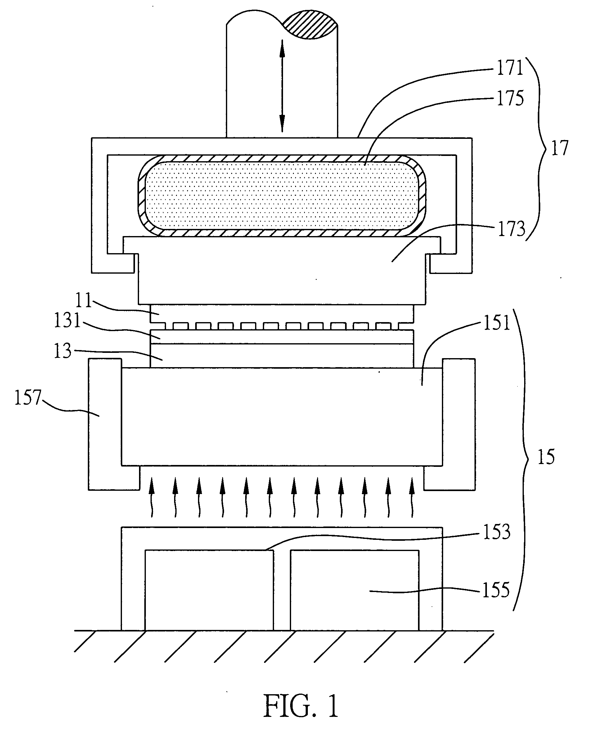
[0044]FIG. 2 is a schematic diagram of the microimprint / nanoimprint device according to a second preferred embodiment of the present invention, wherein same or similar elements as or to those in the first embodiment are designated with same or similar reference numerals and detailed descriptions thereof are omitted for the sake of clarify.

[0045] The second embodiment primarily differs from the first embodiment in that, the first embodiment uses an energy transferring module comprising two energy sources arranged at the same side, but the second embodiment uses an energy transferring module comprising two energy sources arranged at different sides for example at opposite sides.

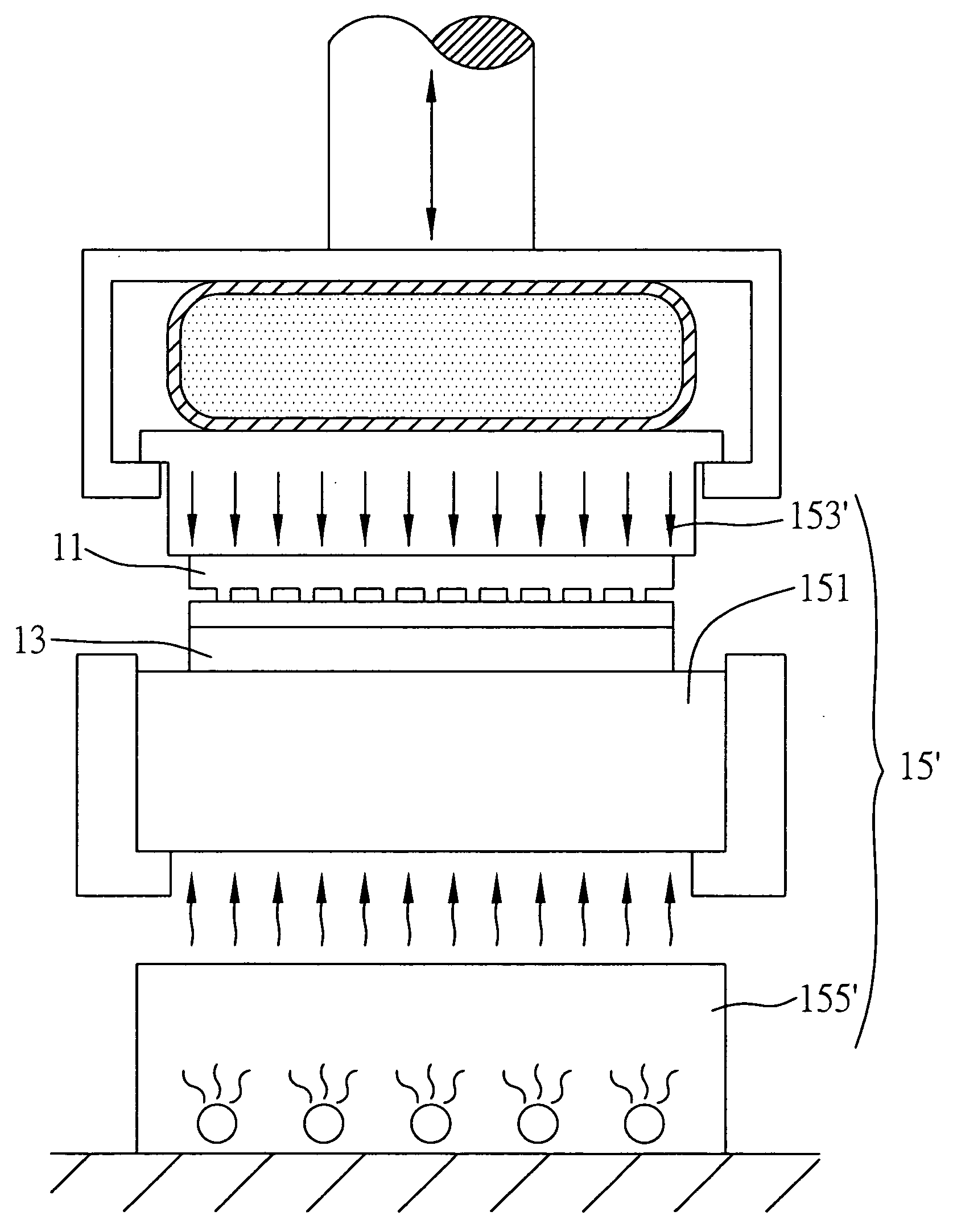
[0046] As shown in FIG. 2, the microimprint / nanoimprint device in this embodiment comprises a mold 11, a substrate 13 and an energy transferring module 15′. The energy transferring module 15′ comprises the energy transferring member 151, an energy source 153′ and an energy source 155′, wherein the energy sour...

third preferred embodiment

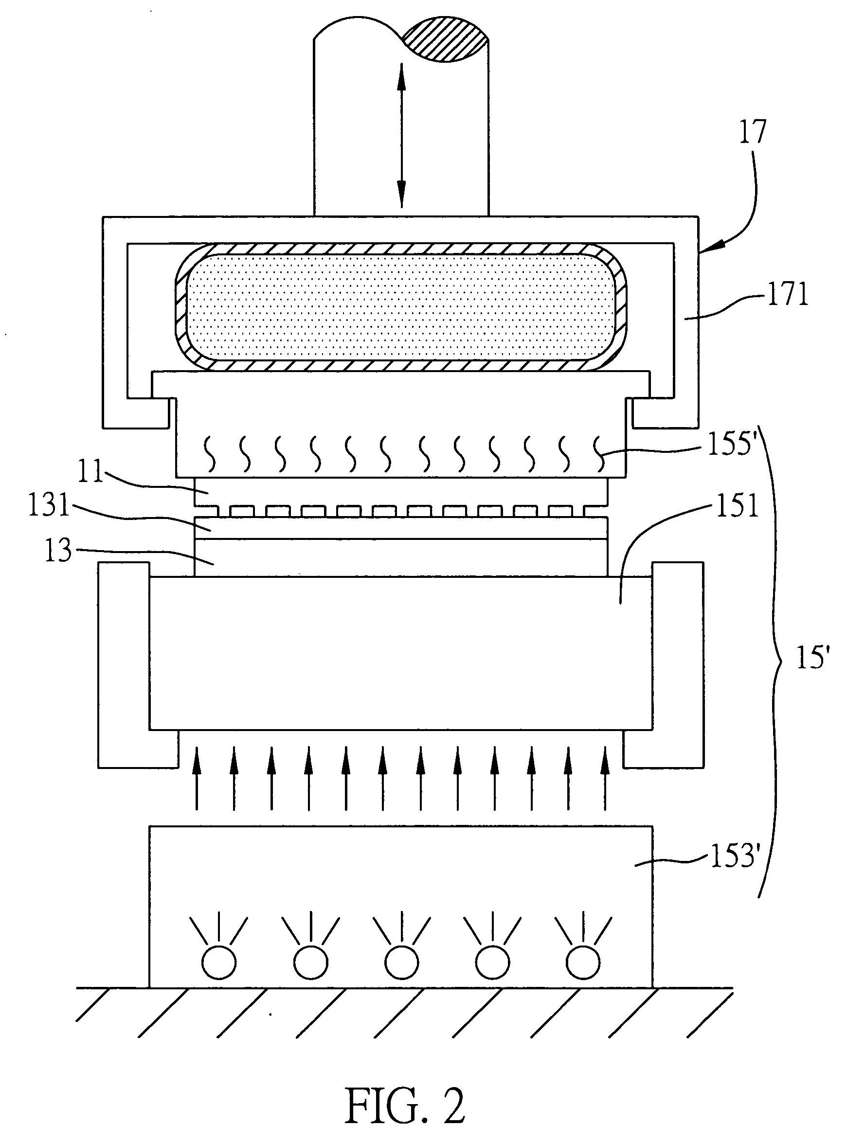
[0048]FIG. 3 is a schematic diagram of the microimprint / nanoimprint device according to a third preferred embodiment of the present invention, wherein same or similar elements as or to those in the first embodiment are designated with same or similar reference numerals and detailed descriptions thereof are omitted.

[0049] The third embodiment primarily differs from the second embodiment in that, in the second embodiment, the energy source 153′ such as an ultraviolet source is located under the energy transferring member 151 and the energy source 155′ such as a heating source is located on the mold 11; however in the third embodiment, positions of the energy source 153′ and the energy source 155′ in the second embodiment are exchanged.

[0050] As shown in FIG. 3, in this embodiment, the energy source 155′ such as a heating source of the energy transferring module 15′ is provided under the energy transferring member 151, and the energy source 153′ such as an ultraviolet source is provi...


PUM

PropertyMeasurementUnit
Sizeaaaaaaaaaa
Frequencyaaaaaaaaaa
Wavelengthaaaaaaaaaa

Abstract

A microimprint / nanoimprint device includes a mold, a substrate and an energy transferring module. The substrate is disposed oppositely to the mold and at least has a molding material layer. The energy transferring module includes an energy transferring member and at least one energy source, wherein the energy transferring member is connected to the substrate or the mold, and the energy source provides imprint energy to the substrate or the mold, such that at least part of the imprint energy goes through the energy transferring member to the substrate or the mold for performing imprint molding.

Description

FIELD OF THE INVENTION [0001] The present invention relates to imprint devices, and more particularly, to a microimprint / nanoimprint device. BACKGROUND OF THE INVENTION [0002] In the past decade, the semiconductor industry has played a very important role in the global economy, by which exploitation and application of various kinds of micro electro mechanical products are promoted along with development of the semiconductor technology. However, as the line width and line pitch processed for various kinds of products are continuously decreased to smaller than 100 nanometers, the current photo-lithography technology encounters a physical problem in optical imaging, and the fabrication difficulty and costs of fabrication equipment are also greatly increased. Although a next-generation lithography technology has been proposed, it still has problems of high equipment costs and low yields. Consequently, the most popular lithography technology at present is nanoimprint lithography (NIL) te...

Claims


Application Information

Patent Timeline
IPC IPC(8): B29C35/08B81C99/00
CPCB29C35/02B29C59/022B29C2035/0827B29C2059/023B82Y10/00B82Y40/00G03F7/0002
Inventor HO, YU-LUNCHEN, LAI-SHENGWANG, WEI-HANWU, JEN-HUACHEN, CHUAN-FENGCHEN, SHOU-REN
Owner IND TECH RES INST
Features
  • Generate Ideas
  • Intellectual Property
  • Life Sciences
  • Materials
  • Tech Scout
  • Unparalleled Data Quality
  • Higher Quality Content
  • 60% Fewer Hallucinations
Learn More