Photomask, manufacturing method thereof, and manufacturing method of electronic device

Inactive Publication Date: 2006-09-14
SEIKO EPSON CORP
View PDF8 Cites 2 Cited by
  • Summary
  • Abstract
  • Description
  • Claims
  • Application Information

AI Technical Summary

Benefits of technology

[0032] According to the method of manufacturing an electronic device, it can provide an electronic device capable of fl

Problems solved by technology

Since, in the conventional method, a request for pattern formation, correction, alteration and the like involves redoing the entire photolithographic process starting from correcting the reticle and manufacturing a new photomask, considerable time and cost are expended.
However, when forming a light-

Method used


Image

  • Photomask, manufacturing method thereof, and manufacturing method of electronic device
  • Photomask, manufacturing method thereof, and manufacturing method of electronic device
  • Photomask, manufacturing method thereof, and manufacturing method of electronic device

Examples


first embodiment

[0045] The first embodiment of the present invention shall be explained below with reference to the accompanying drawings.

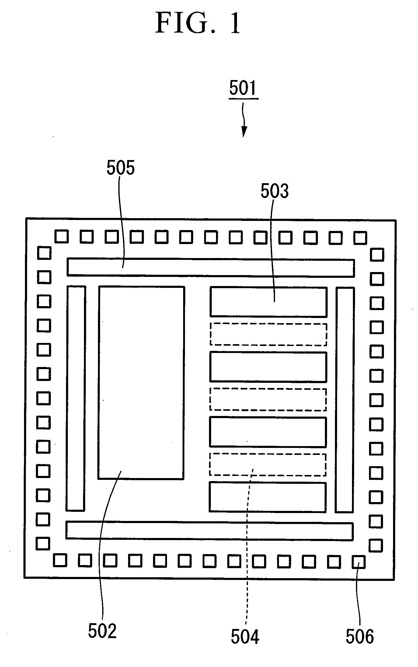
[0046]FIG. 1 is an outline lineblock diagram showing a semiconductor device produced using the photomask of the present embodiment. As an example of a semiconductor device, the present embodiment explains the creation of a driving LSI for a liquid crystal display, which is a kind of Application Specific Integrated Circuit (ASIC).

[0047] As shown in FIG. 1, a semiconductor device 501 of the present embodiment includes a memory portion 502 including ROM (read-only memory) and RAM (random-access memory), a plurality of logic circuit portions 503 that consist of a plurality of MOS transistors, a wiring portion 504 (wiring region) in which a number of wirings that connect the memory portion 502 and the plurality of logic circuit portions 503 are disposed, an input / output gate portion 505, and an external terminal 506. The light-shielding pattern density of the wiring...

second embodiment

[0070] The second embodiment of the present invention shall be explained below with reference to the accompanying drawings.

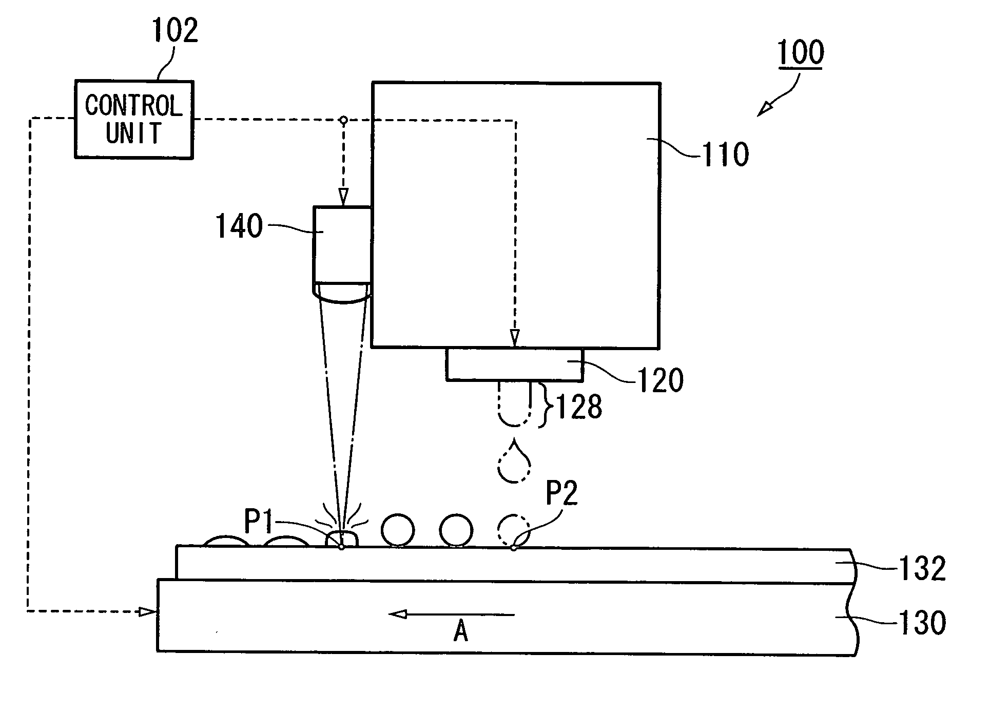
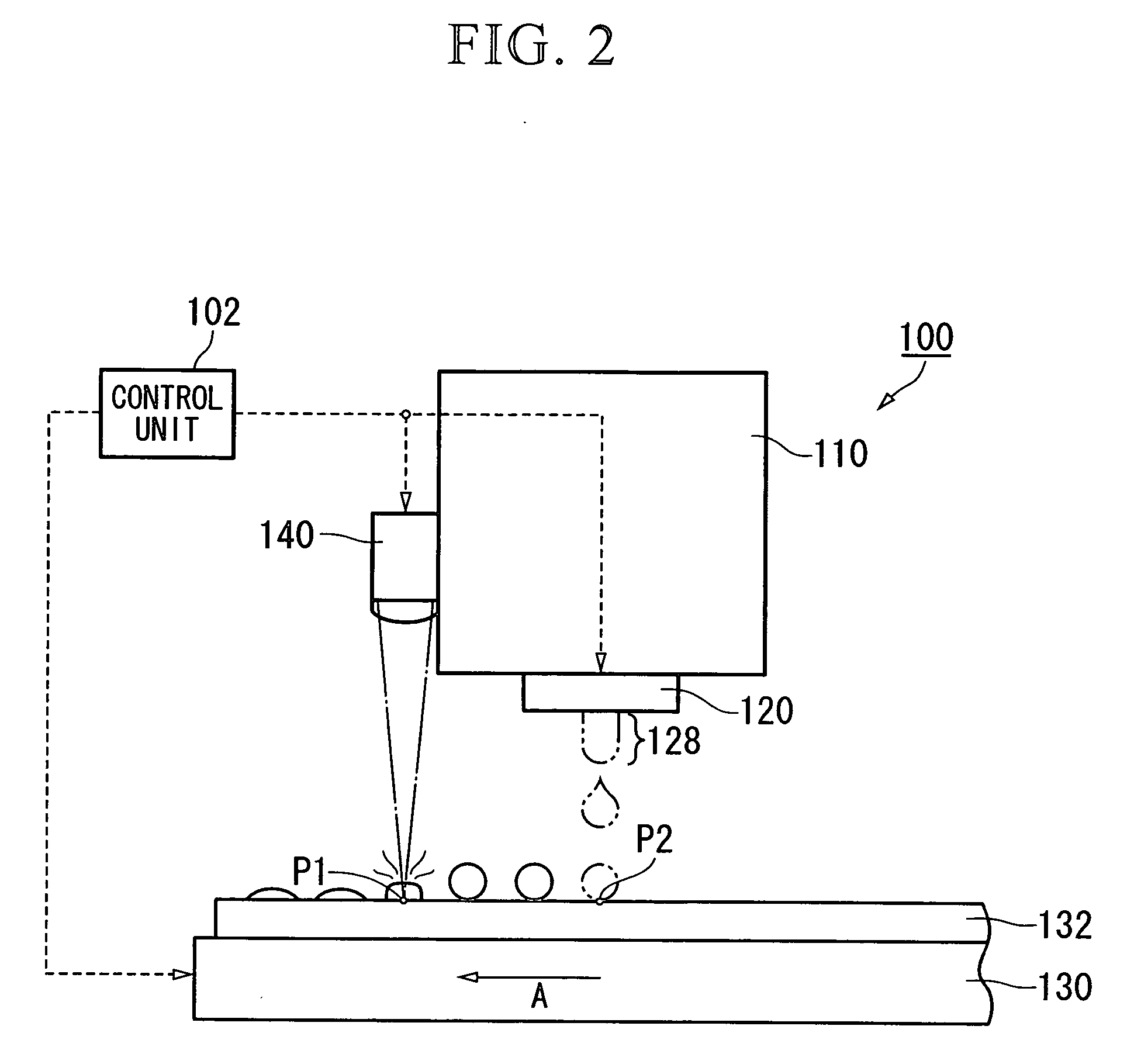
[0071] In the first embodiment, a description was given for the pattern formation apparatus 100 that applied droplets containing a light-shielding material, and then irradiated the droplets with a low-intensity laser light to dry the droplets and form a light-shielding pattern. In contrast, the second embodiment describes a pattern formation apparatus that dries droplets by irradiating them with laser light approximately simultaneously with the application of the droplets. In the pattern formation apparatus of the present embodiment, the same reference numerals are used to designate elements identical to those in the first embodiment.

[0072]FIG. 6 is a lineblock diagram of the pattern formation apparatus 200 in connection with the second embodiment.

[0073] As shown in FIG. 6, compared with the pattern formation apparatus 100 of the first embodiment, a reflector...

third embodiment

[0076] The third embodiment of the present invention shall be explained below with reference to the accompanying drawings.

[0077] The first and second embodiments described a pattern formation apparatus that produced a light-shielding pattern by radiating laser light on droplets containing a light-shielding material and drying the droplets. In contrast, the third embodiment describes a pattern formation apparatus that guides the path of the droplets by laser light irradiation.

[0078]FIG. 7 is a lineblock diagram of the pattern formation apparatus 10. A control unit 5 controls the operation of each part of the pattern formation apparatus 10.

[0079] A solution tank 3 stores a solution consisting of chromium particles distributed in n-tetradecane in the form of a liquid, similarly to the first and second embodiments. The solution held in the solution tank is supplied to an ejection portion 25 through a pipe 4, and then ejected from the nozzle of the ejection portion 25. The pattern for...


PUM


Abstract

A method of manufacturing a photomask includes: ejecting droplets of a liquid containing a light-shielding material at predetermined positions on a substrate using a droplet ejection method, and drying the liquid to form a light-shielding pattern on the substrate, the light-shielding pattern containing the light-shielding material.

Description

CROSS-REFERENCE TO RELATED APPLICATION [0001] This application claims priority to Japanese Patent Application No. 2005-066091, filed Mar. 9, 2005, the contents of which are incorporated herein by reference. BACKGROUND [0002] 1. Technical Field [0003] The present invention relates to a photomask, a method of manufacturing the same, and a method of manufacturing an electronic device, and particularly relates to a method of manufacturing a photomask using a droplet ejection method. [0004] 2. Related Art [0005] In the manufacturing process for electronic equipment such as semiconductor devices and various displays, photolithographic techniques have conventionally been used for producing thin-film patterns, with a method being adopted of transferring a photoresist pattern onto a photosensitive material such as a photoresist applied on a substrate. [0006] A common procedure of manufacturing a photomask is to manufacture a master mask by repeating reduced projection exposure after forming ...

Claims


Application Information

Patent Timeline
IPC IPC(8): B41J2/01G03F1/68G03F1/76
CPCB41J2/01G03F1/54G03F1/56G03F1/68G03F1/38H05K3/125
Inventor MIURA, HIROTSUNA
Owner SEIKO EPSON CORP
Why Eureka
Try Eureka