

Semiconductor, functional device, electrochromic device, optical device, and image-taking unit
a functional device and semiconductor technology, applied in the field of semiconductor/solid-state device details, camera filters, semiconductors, etc., can solve the problems of insufficient control of the flat band potential, inability to use expensive and/or dangerous semiconductor materials, and insufficient prevention of reverse curren
- Summary
- Abstract
- Description
- Claims
- Application Information
AI Technical Summary
Benefits of technology
Problems solved by technology
Method used
Image

Examples
example 1
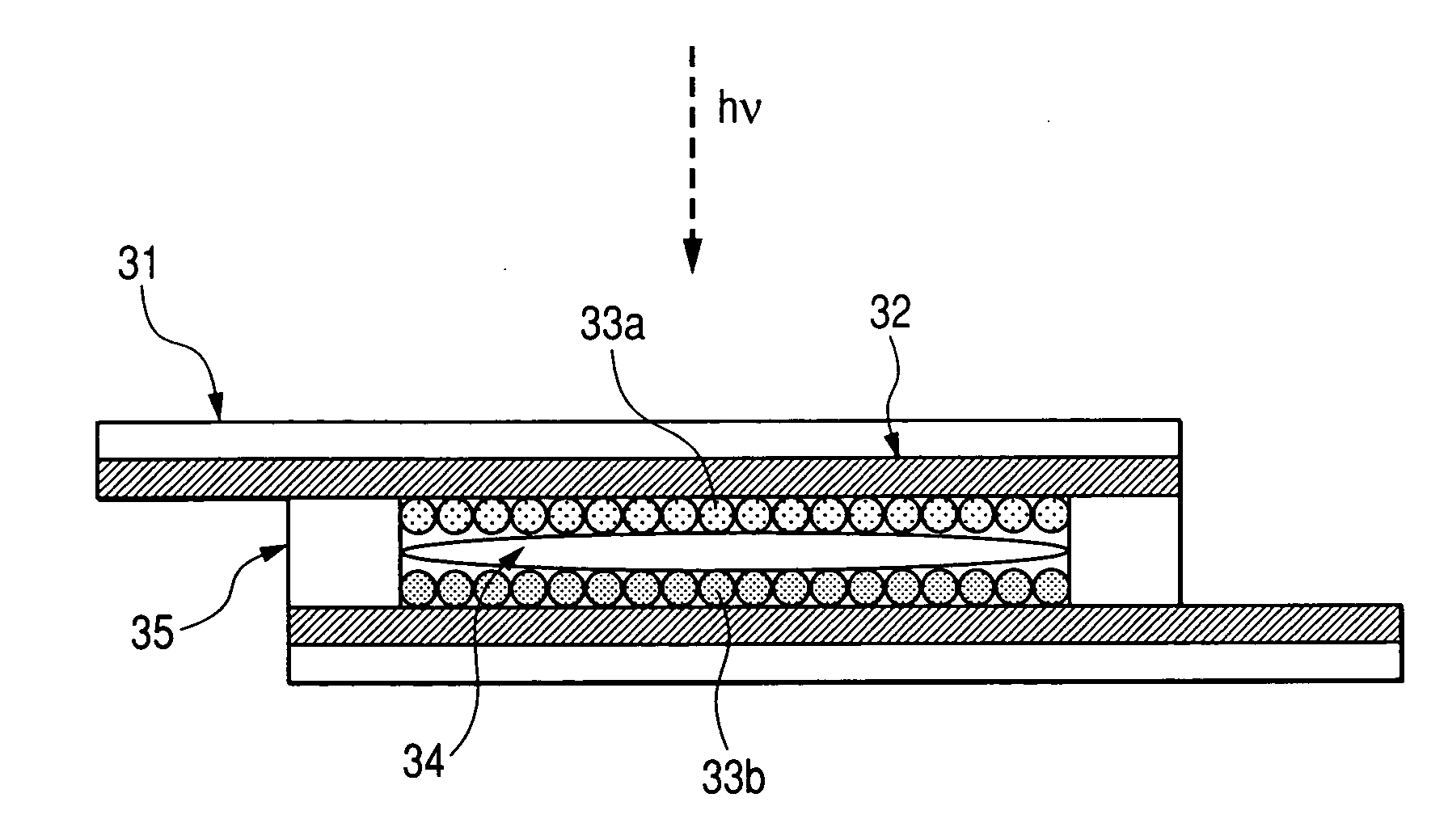
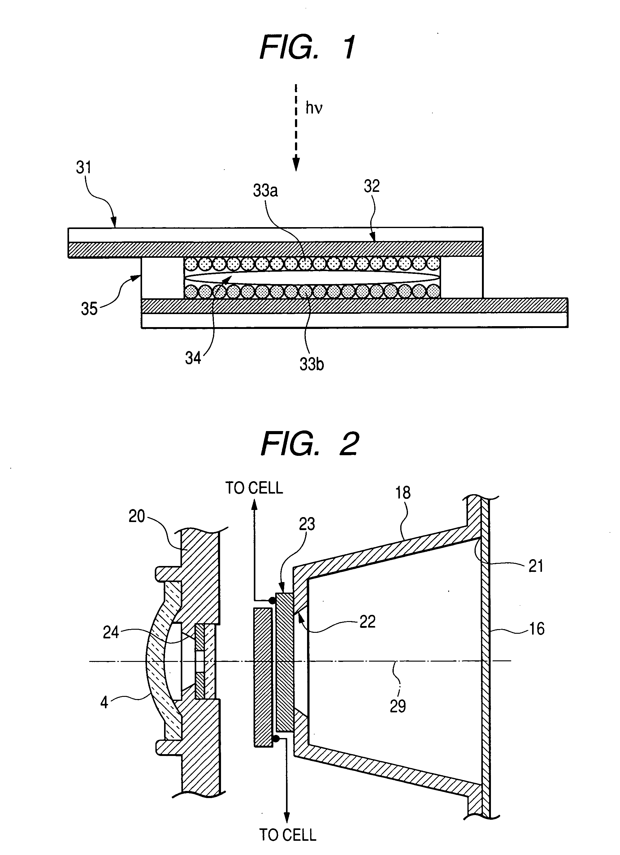
[0156] Polyethyleneglycol (molecular weight: 20,000) was added to an aqueous dispersion of tin oxide having an average diameter of 5 nm, and uniformly stirred to prepare a coating solution. As a substrate to be coated, an ITO conductive glass (thickness: 0.7 mm) provided with an anti-reflection film was used. The coating solution was uniformly applied on the ITO film of the transparent conductive glass. After the application, the glass was heated up to 450° C. over a time period of 100 minutes, and baking was carried out at 450° C. for 30 minutes to remove polymer. The application and the baking were repeated until the total amount of the applied tin oxide reached 7 g / m2, to obtain a tin oxide nanoporous electrode having a uniform thickness. The electrode prepared in the above-described manner had a surface roughness coefficient of about 400.
[0157] A 0.04 mol / L aqueous solution was prepared for each of compounds Nos. 1 to 4 described below. The tin oxide nanoporous electrode as pre...
example 2
[0163] Methods for preparing a sample 202 (present invention) of the electrochromic device according to the present invention and a sample 201 (comparative example) will be described.
[0164] (1) Preparation of Sample 201 (Comparative Example)
[0165] The sample 201 (comparative example) was prepared in the following procedure: (i) application of nanoparticulate tin oxide for cathode, (ii) application of nanoparticulate tin oxide for anode, (iii) adsorption of electrochromic dyes, and (iv) assembly of an electrochromic device, in this order.
[0166] (i) Application of Nanoparticulate Tin Oxide for Cathode
[0167] Polyethyleneglycol (molecular weight: 20,000) was added to an aqueous dispersion of tin oxide having a diameter of about 40 nm, and uniformly stirred to prepare a coating solution. As a substrate to be coated, an ITO conductive glass (thickness: 0.7 mm) having an anti-reflection film on the rear side was used. The coating solution was uniformly applied onto the ITO film of the ...
example 3
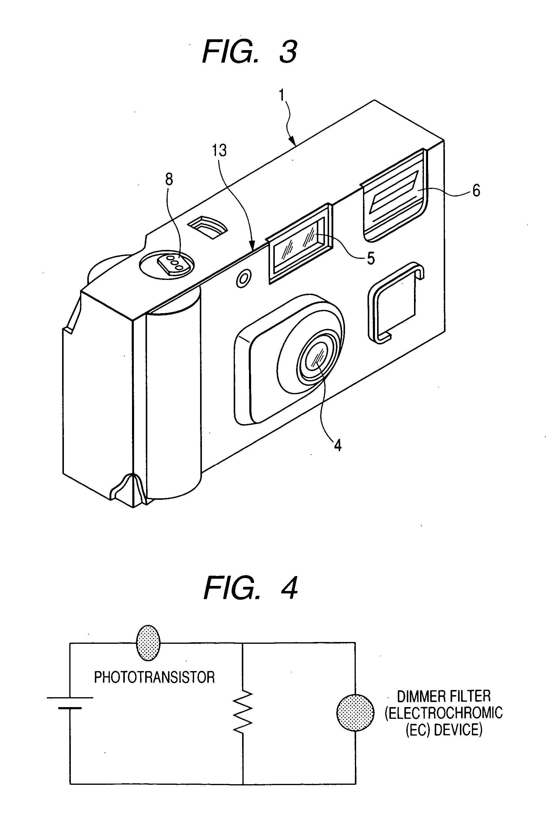
[0182] An example in which the electrochromic device sample 202 of the present invention is incorporated into a lens-combined film, will be described.
[0183] As illustrated in FIGS. 2 and 3, a lens-combined film in this example includes (1) a dimmer filter 23 (an electrochromic device) and (2) a phototransistor 13 (an electromagnetic wave sensor). The phototransistor 13 is provided external to the unit to generate electromotive force in accordance with the illuminance of external light, so that the dimmer filter 23 can be colored by the electromotive force to control the intensity of light reaching a color negative film 16.
[0184] (1) Electrochromic Device Sample 202
[0185] The electrochromic device sample 202 prepared in Example 2 was used.
[0186] (2) Circuitry of the Electrochromic Device
[0187] As the electromagnetic wave sensor, a phototransistor (PT380, manufactured by Sharp Corp.), and as the electromotive force-generating element, a dry cell (AA size: 1.5 V) for a strobe of t...
PUM
 Abstract
Description
Claims
Application Information