Method for manufacturing organic electroluminescence display

a manufacturing method and technology for electroluminescence display, applied in the manufacture of electrode systems, instruments, electric discharge tubes/lamps, etc., can solve the problems of short circuit between, reduced thickness of organic light-emitting layer, and complicated manufacturing process of organic el display

Inactive Publication Date: 2006-09-14
DAEWOO ELECTRONICS CO LTD
View PDF2 Cites 12 Cited by
  • Summary
  • Abstract
  • Description
  • Claims
  • Application Information

AI Technical Summary

Benefits of technology

[0036] It is, therefore, an object of the present invention to provide a method for manufacturing an organic electroluminescence display, capable of forming both a

Problems solved by technology

In this connection, when the organic light-emitting layer is deposited on the anode layer in the openings, there is a likelihood that the thickness of the organic light-emitting layer is reduced near the separator because of a shadow effect due to the separator, thus causing a short circuit between the cathode layer deposited on top of the organic light-emitting layer and the underneath anode layer.
Therefore, the manufacturing process for the organic EL display becomes complicated and manufacturing costs increases.
Furthermore, since the insulating layer and the separator are respectively formed on top of each other as separate layers, adhesiveness therebetween may be weak.
Thus, in case a ratio of width to height of a device isolation structure including the insulating layer and the separator decreases, the device isolation structure may be broken.
The method in Reference 2, however, also has disadvantages in that manufacturing costs for the organic EL display increases g

Method used


Image

  • Method for manufacturing organic electroluminescence display
  • Method for manufacturing organic electroluminescence display
  • Method for manufacturing organic electroluminescence display

Examples


Embodiment Construction

[0047] Hereinafter, preferred embodiment of the present invention will be described in detail with reference to the accompanying drawings.

[0048] In the drawings, thickness of various layers and regions therein are enlarged for the clear illustration thereof. Like reference numerals designate the same or corresponding parts in the various drawings.

[0049] A method for manufacturing an organic electroluminescence (EL) display will be explained in detail in accordance with preferred embodiments of the present invention in connection with the accompanying drawings.

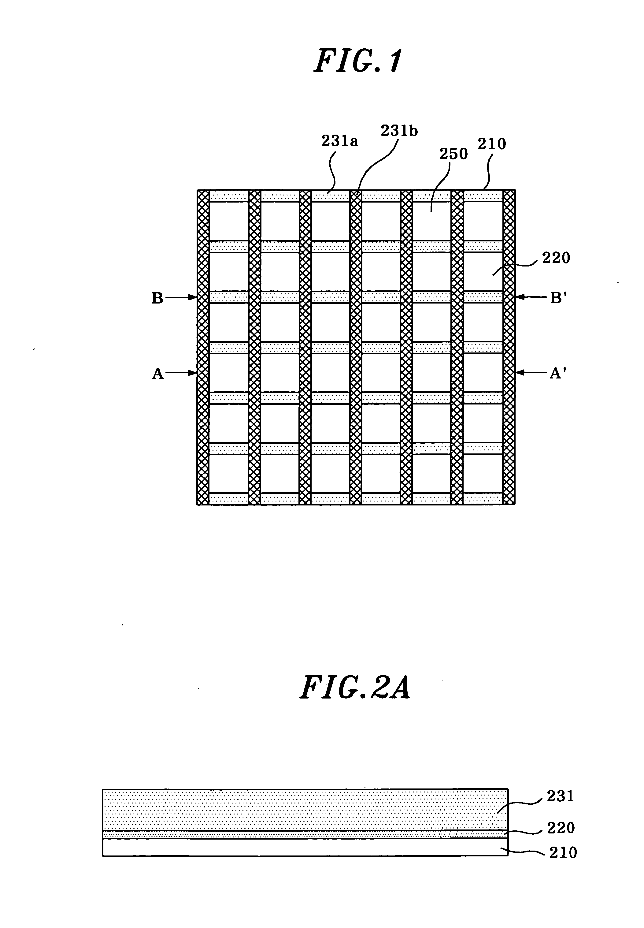
[0050] Referring to FIG. 1, there is shown an organic EL display fabricated in accordance with a first, a second or a third preferred embodiment of the present invention.

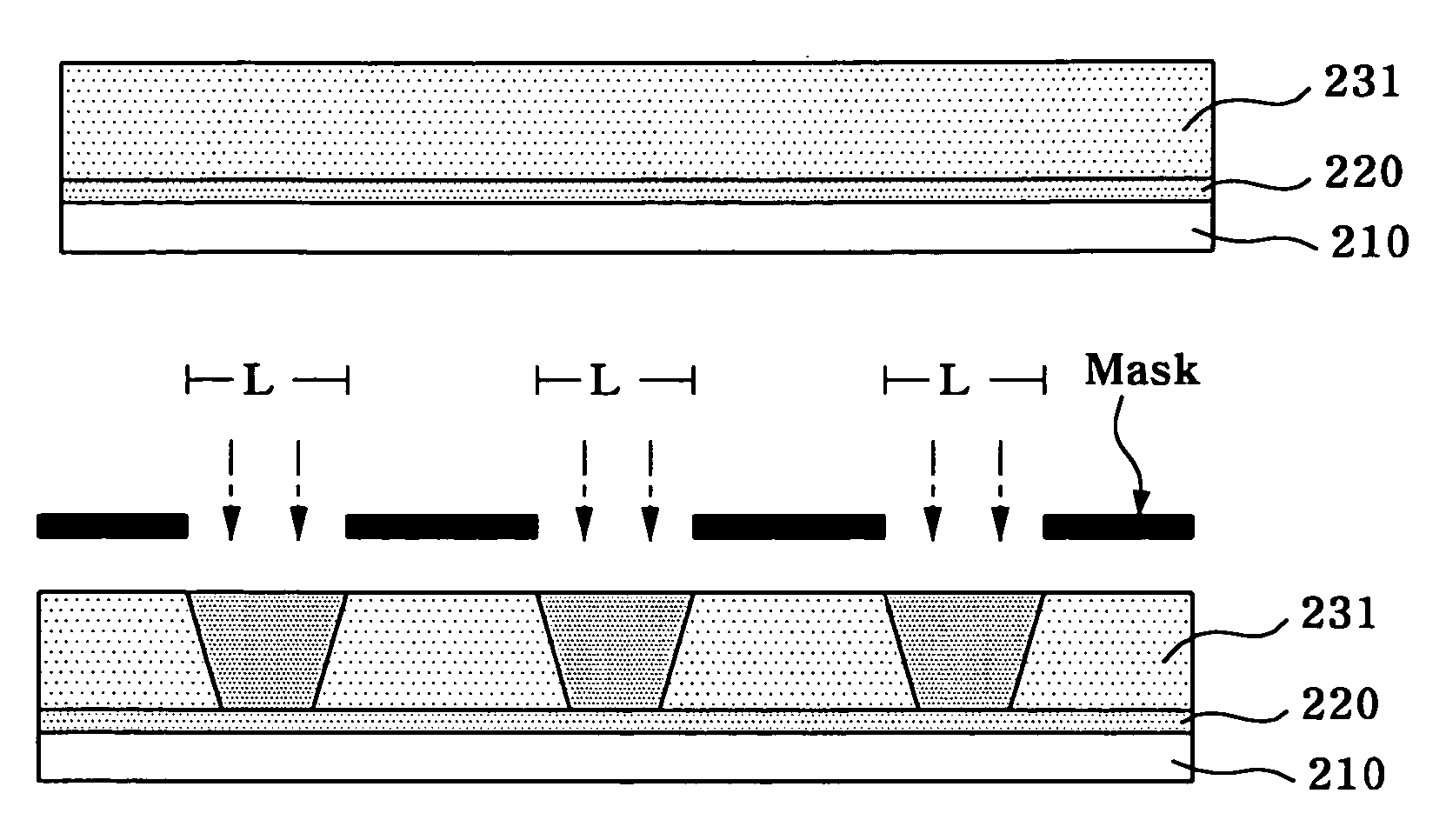
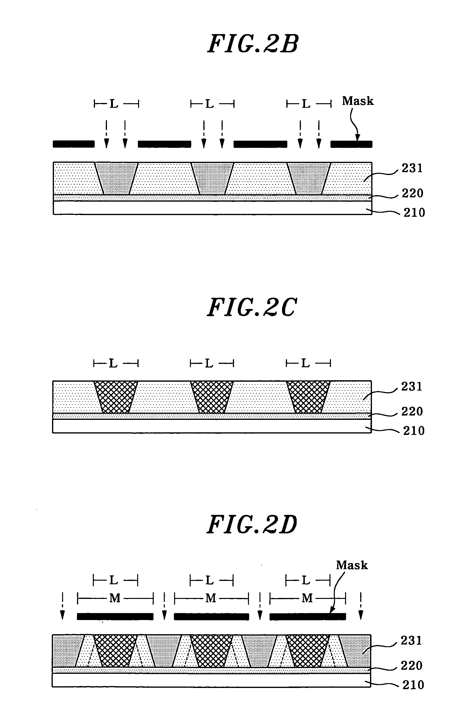
[0051] As shown in FIG. 1, a plurality of first electrodes 220, which are made of indium tin oxide (ITO), indium-doped zinc oxide (IZO or IXO), or the like, is patterned on a transparent substrate 210 in the shape of stripes. An insulating layer 231a of a l...


PUM


Abstract

A method for manufacturing an organic electroluminescence display includes forming a plurality of first electrodes on a substrate in a shape of stripe; forming a photoresist layer on an entire surface of the substrate; performing a first exposure of a first area on the photoresist layer crossing the first electrodes; carrying out an image reversal of the first exposed photoresist layer; performing a second exposure of a remaining area on the photoresist layer except a second area crossing the first electrodes and a third area between the first electrodes; performing a third exposure of the entire surface of the photoresist layer; and developing the second exposed photoresist layer and the third exposed photoresist layer.

Description

[0001] This application is a Continuation Application of PCT International Application No. PCT / KR2005 / 004064 filed on Nov. 30, 2005, which designated the United States.FIELD OF THE INVENTION [0002] The present invention relates to a method for manufacturing an organic electroluminescence display through a simplified manufacturing process. BACKGROUND OF THE INVENTION [0003] In general, an organic electroluminescence (hereinafter referred to as an EL) display is one of flat plate type displays. The organic EL display includes an anode layer and a cathode layer formed on a transparent substrate, and an organic light-emitting layer is interposed between the anode layer and the cathode layer. The organic EL display has very thin thickness and it is fabricated as a matrix pattern. [0004] Such an organic EL display is driven at a low voltage not greater than 15 Volts, and it exhibits advanced characteristics in terms of brightness, viewing angle, response time, power consumption, and so fo...

Claims


Application Information

Patent Timeline
IPC IPC(8): H01J9/227
CPCH01L27/3283H01L51/56H10K59/173H10K71/00H05B33/10H05B33/22
Inventor CHOI, KYUNG HEEBYUN, BYUNG HYUNYI, SEUNG JUN
Owner DAEWOO ELECTRONICS CO LTD
Why Eureka
Try Eureka