Film formation method and apparatus for semiconductor process

a film formation method and semiconductor technology, applied in the field of film formation methods and apparatus for semiconductor processes, can solve the problems of low film thickness controllability of the process, unsuitability of thermal cvd process at high temperature, and inability to meet the requirements of film thickness control, etc., and achieve the effect of high film thickness controllability

Active Publication Date: 2006-09-14
TOKYO ELECTRON LTD
View PDF14 Cites 321 Cited by
  • Summary
  • Abstract
  • Description
  • Claims
  • Application Information

AI Technical Summary

Benefits of technology

[0014] An object of the present invention is to provide a method and apparatus for forming an insulating film, which can employ a relatively low process temperature in film formation, and cause the film to be etched by a low amount during a cleaning process, so that the cleaning process can be performed with high controllability in the film thickness, while allowing the film to sufficiently serve as an etching stopper film or inter-level insulating film. It should be noted that the present invention is a modification of the invention disclosed in Jpn. Pat. Appln. KOKAI Publication No. 2003-282566 (Oct. 3, 2003).

Problems solved by technology

However, where a thin film having a low heat resistance is present as an underlayer, a thermal CVD process at high temperature is unsuitable.
Accordingly, the insulating film may be excessively etched by cleaning, and thus the cleaning process entails lower controllability in the film thickness.
However, the conventional film formation method cannot satisfy this requirement.

Method used


Image

  • Film formation method and apparatus for semiconductor process
  • Film formation method and apparatus for semiconductor process
  • Film formation method and apparatus for semiconductor process

Examples


first embodiment

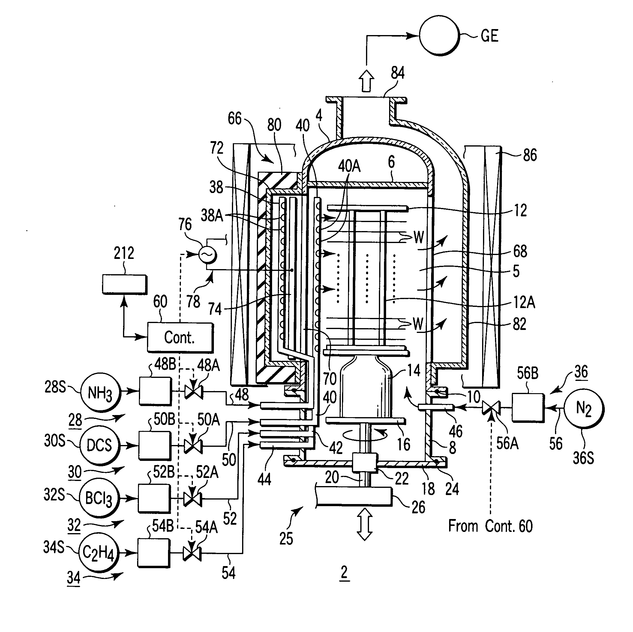
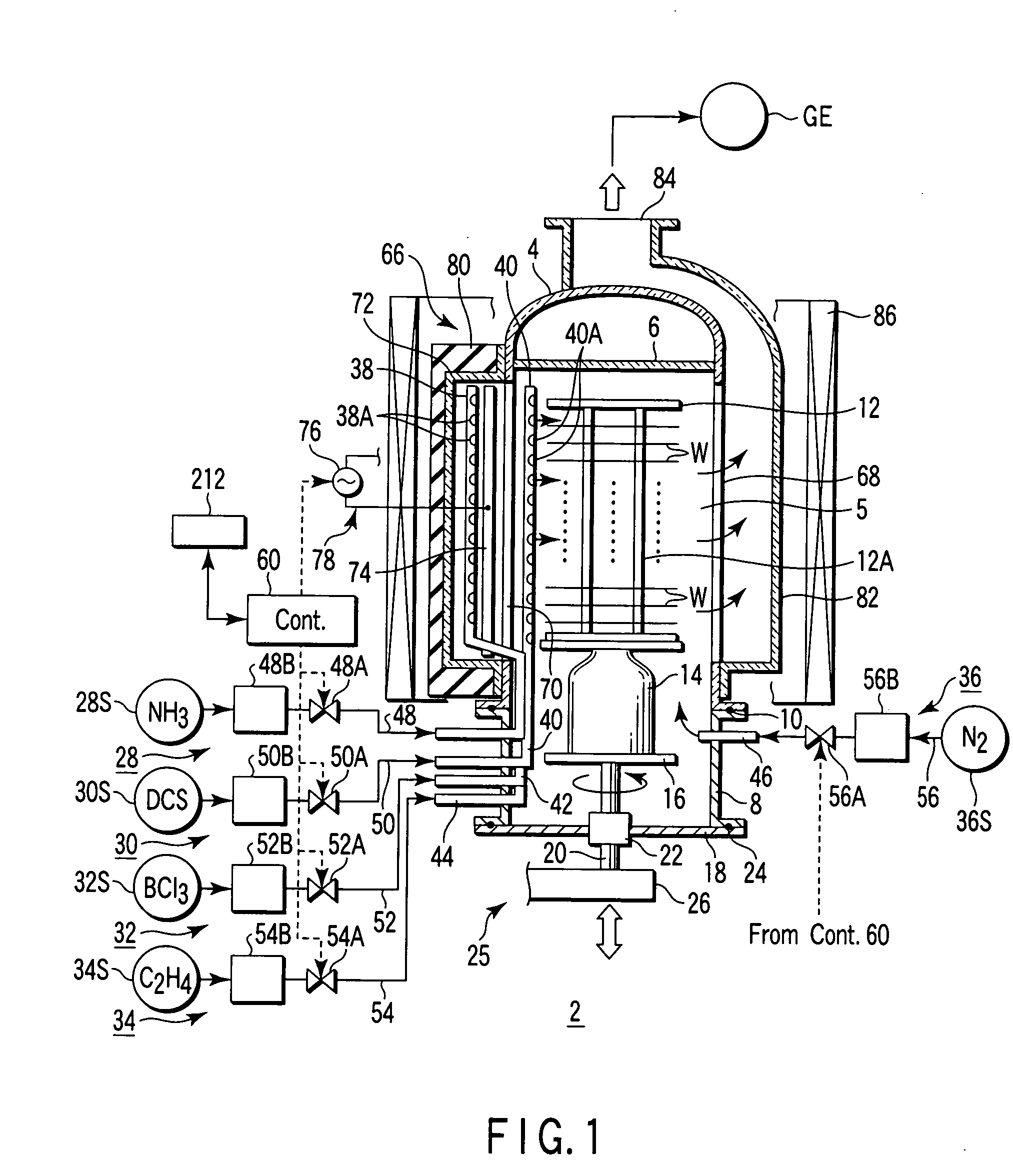
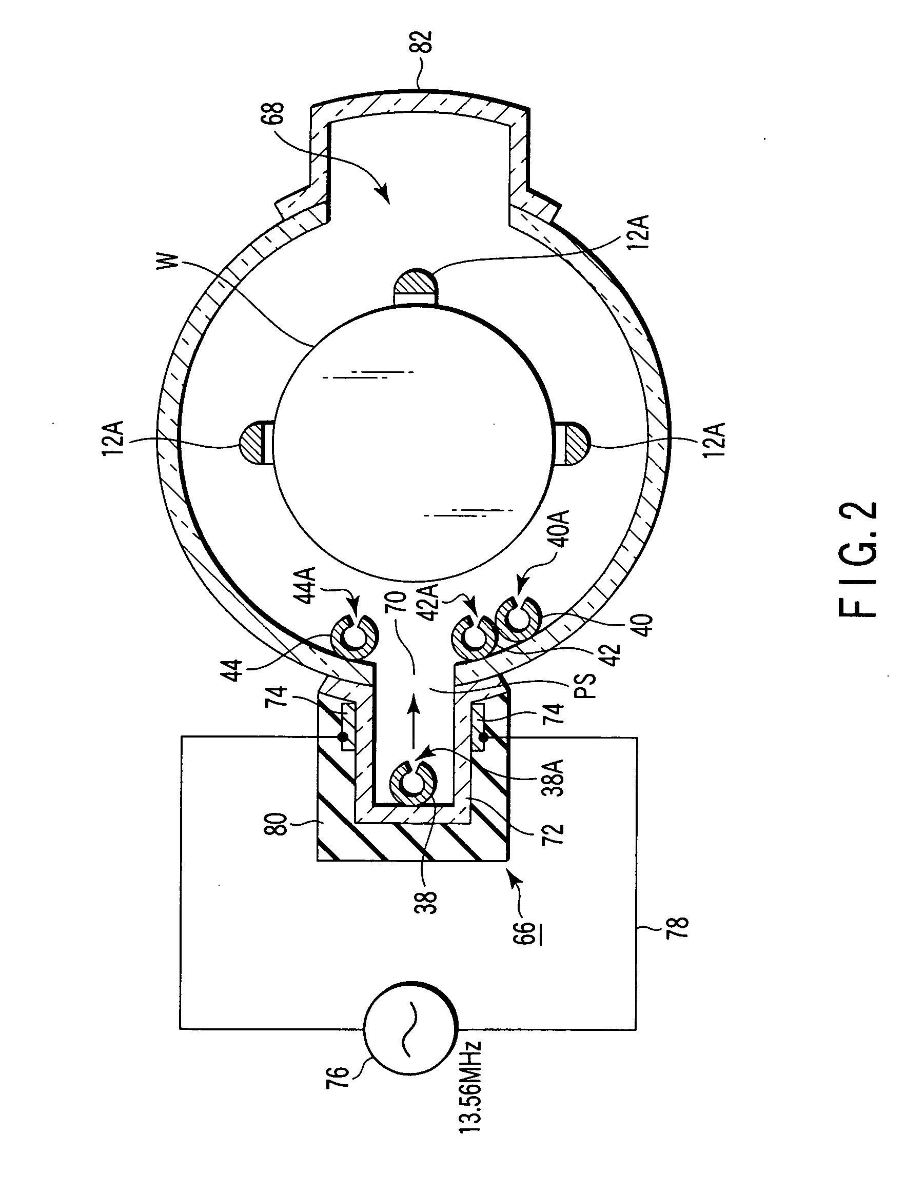
[0095] In the film formation method according to a first embodiment, an insulating film of SiBCN (boron doped silicon carbon nitride) is formed on semiconductor wafers by CVD. In order to achieve this, a first process gas containing dichlorosilane (DCS) gas as a silane family gas, a second process gas containing ammonia (NH3) gas as a nitriding gas, a third process gas containing C2H4 gas (ethylene gas) as a carbon hydride gas, and a fourth process gas containing BCl3 gas as a boron-containing gas are selectively supplied into the process field 5 accommodating wafers W.

[0096] At first, the wafer boat 12 at room temperature, which supports a number of, e.g., 50 to 100, wafers having a diameter of 300 mm, is loaded into the process container 4 heated at a predetermined temperature, and the process container 4 is airtightly closed. Then, the interior of the process container 4 is vacuum-exhausted and kept at a predetermined process pressure, and the wafer temperature is increased to a...

second embodiment

[0112] In the film formation method according to a second embodiment, an insulating film of SiCN (silicon carbon nitride undoped with boron) is formed on semiconductor wafers by CVD. In order to achieve this, the first process gas containing dichlorosilane (DCS) gas as a silane family gas, the second process gas containing ammonia (NH3) gas as a nitriding gas, and the third process gas containing C2H4 gas (ethylene gas) as a carbon hydride gas are selectively supplied into the process field 5 accommodating wafers W.

[0113] Specifically, in the second embodiment, the method according to the first embodiment shown in FIG. 3 is modified to exclude supply of the fourth process gas containing BCl3 gas as a boron-containing gas, in performing film formation. Accordingly, the fourth process gas supply circuit 32 of the film formation apparatus shown in FIG. 1 is not needed to implement the second embodiment. The second embodiment employs the same process conditions as those of the first em...

third embodiment

[0117] In the film formation method according to a third embodiment, an insulating film of BCN (boron doped carbon nitride) is formed on semiconductor wafers by CVD. In order to achieve this, the second process gas containing ammonia (NH3) gas as a nitriding gas, the third process gas containing C2H4 gas (ethylene gas) as a carbon hydride gas, and the fourth process gas containing BCl3 gas as a boron-containing gas are selectively supplied into the process field 5 accommodating wafers W.

[0118] Specifically, in the third embodiment, the method according to the first embodiment shown in FIG. 3 is modified to exclude supply of the first process gas containing dichlorosilane (DCS) gas as a silane family gas, in performing film formation. Accordingly, the first process gas supply circuit 30 of the film formation apparatus shown in FIG. 1 is not needed to implement the third embodiment. The third embodiment employs the same process conditions as those of the first embodiment except for c...


PUM

PropertyMeasurementUnit
diameteraaaaaaaaaa
frequencyaaaaaaaaaa
frequencyaaaaaaaaaa

Abstract

An insulating film is formed on a target substrate by CVD, in a process field to be selectively supplied with a first process gas containing a silane family gas, a second process gas containing a nitriding or oxynitriding gas, and a third process gas containing a carbon hydride gas. This method alternately includes first to fourth steps. The first step performs supply of the first and third process gases to the field while stopping supply of the second process gas to the process field. The second step stops supply of the first to third process gases to the field. The third step performs supply of the second process gas to the field while stopping supply of the first and third process gases to the field. The fourth step stops supply of the first to third process gases to the field.

Description

CROSS-REFERENCE TO RELATED APPLICATIONS [0001] This application is based upon and claims the benefit of priority from prior Japanese Patent Applications No. 2005-066340, filed Mar. 9, 2005; and No. 2006-004191, filed Jan. 11, 2006, the entire contents of both of which are incorporated herein by reference.BACKGROUND OF THE INVENTION [0002] 1. Field of the Invention [0003] The present invention relates to a film formation method and apparatus for a semiconductor process for forming an insulating film on a target substrate, such as a semiconductor wafer. The term “semiconductor process” used herein includes various kinds of processes which are performed to manufacture a semiconductor device or a structure having wiring layers, electrodes, and the like to be connected to a semiconductor device, on a target substrate, such as a semiconductor wafer or a glass substrate used for an LCD (Liquid Crystal Display) or FPD (Flat Panel Display), by forming semiconductor layers, insulating layers,...

Claims


Application Information

Patent Timeline
Patent Type & Authority Applications(United States)
IPC IPC(8): H01L21/31H01L21/469
CPCC23C16/36C23C16/45523C23C16/45578C23C16/515H01L21/3144H01L21/3148H01L21/3185H01L21/76829H01L21/02271H01L21/0228H01L21/02211
Inventor CHOU, PAO-HWAHASEBE, KAZUHIDE
Owner TOKYO ELECTRON LTD
Why Eureka
Try Eureka