Methods for making large dimension, flexible piezoelectric ceramic tapes

a flexible piezoelectric ceramic and tape technology, applied in the direction of mechanical vibration separation, device material selection, instruments, etc., can solve the problems of large sheet, difficult to make a thin, limited piezoelectric ceramic material detection/test system application,

Inactive Publication Date: 2006-09-21
PALO ALTO RES CENT INC
View PDF22 Cites 21 Cited by
  • Summary
  • Abstract
  • Description
  • Claims
  • Application Information

AI Technical Summary

Problems solved by technology

A significant drawback of piezoelectric ceramics is that it is difficult to make a thin, large sheet (at many inches to several feet scale), due to the brittle nature of the material.
Due to this limitation, it cannot be mounted to a curved surface or embedded in a structure which needs to be flexible.
Unfortunately, many real world applications require detecting and testing of curved surfaces and / or flexible structure, thus the mentioned brittleness greatly limits the applications of piezoelectric ceramic materials in detection / test systems.
Unfortunately, the piezoelectric effect of piezoelectric polymers is weak—about one-tenth of piezoelectric ceramics—and the materials are very soft.
However, the fabrication techniques for the SMART layer are labor intensive and restrictive in design choices.
Particularly, the disclosed fabrication process for the SMART layer do not lend itself to obtaining of a flexible tape with high density elements and a variety of geometric shapes for those elements, which in turn permits more versatile functional capabilities.

Method used


Image

  • Methods for making large dimension, flexible piezoelectric ceramic tapes
  • Methods for making large dimension, flexible piezoelectric ceramic tapes
  • Methods for making large dimension, flexible piezoelectric ceramic tapes

Examples


first embodiment

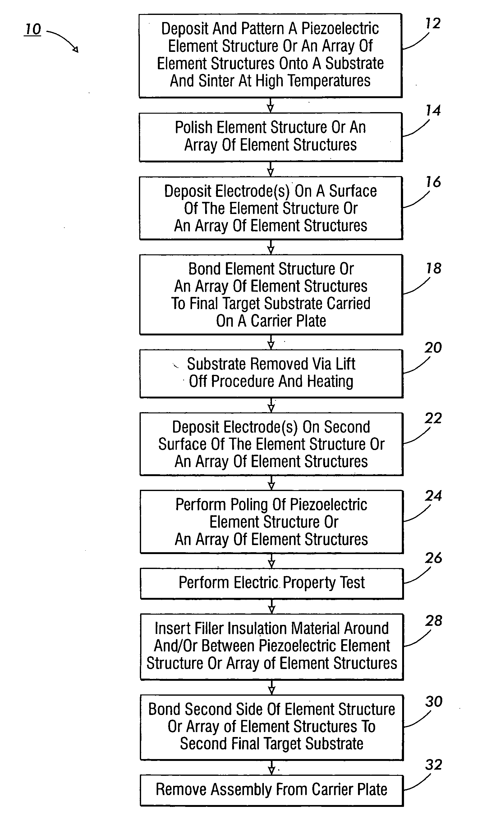
[0042]FIG. 1 illustrates a high level process flow 10 for a manufacturing process according to the concepts of the present application. While the following discussion focuses on producing piezoelectric thick film elements (with thickness between 10 and 100 μm), it is to be appreciated the disclosed processes may be used with other materials and may also be used for production of thin-film elements (with thickness less than 10 μm) and elements with thicknesses greater than 100 μm to millimeter in scale. Also, the following techniques are intended to be applicable to the generation of individual elements and arrays of elements.

[0043] Initially, piezoelectric ceramic thick film elements are fabricated by depositing the piezoelectric material onto an appropriate substrate by use of a direct marking technology 12. In the deposition techniques employed, ceramic type powders are used in a preferred embodiment. The fabrication process includes sintering the material preferably at a temperat...

second embodiment

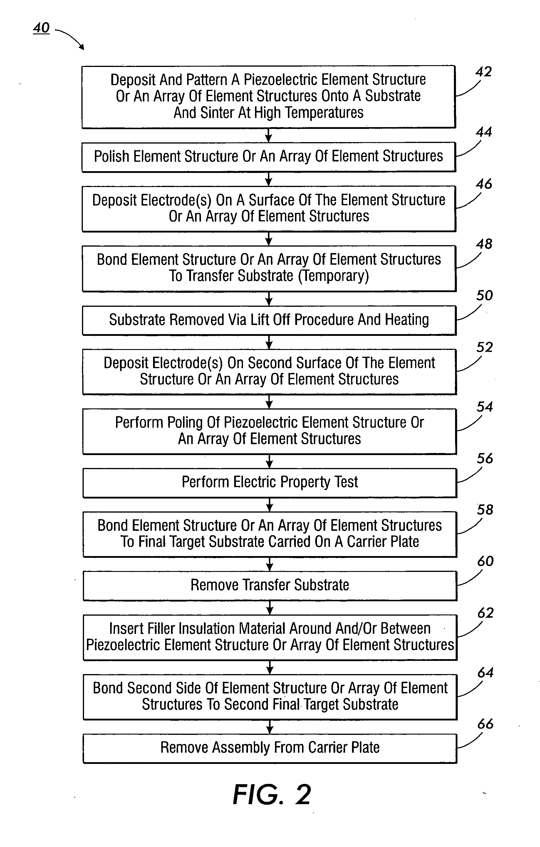
[0045] Turning to FIG. 2, illustrated is a second high-level process flow 40 for the present application. This process differs from FIG. 1 in that the bonding is to a transfer substrate rather than to a final target substrate. Thus, the fabrication step 42, the tape polishing step 44 and the electrode depositing step 46 are performed in the same manner as steps 12, 14 and 16 of FIG. 1. At bonding step 48, the bonding is to a transfer substrate, as this connection is not intended to be permanent. Thereafter, the liftoff step 50, the second electrode deposition step 52, the poling step 54 and electric property test step 56, which correlate to steps 20, 22, 24 and 26 of FIG. 1, are performed.

[0046] The piezoelectric elements are then bonded to a final target substrate 58, in a procedure similar in design to step 18 of FIG. 1. Following bonding step 58, the transfer substrate is removed 60. Thereafter, the steps of inserting an insulative filler 62, bonding to the second final target su...

third embodiment

[0088]FIG. 16 is an A-A sectional view 140. This drawing shows that the density of piezoelectric elements in an area can be changed (i.e., the elements do not need to be evenly distributed in an area), and the piezoelectric elements may be formed in a variety of shapes 142. Thus the function of the piezoelectric tape can be locally adjusted. Filler 144 is distributed around and between the elements.

[0089]FIG. 17 is a polymer tape 150 with a patterned metallization layer 152. Depending on the shape and distribution of the piezoelectric elements, and the design of outside circuits, the metallization layer can be patterned on the polymer tape 150 to connect the piezoelectric elements to external circuits, via circuit lines 154, individually or group by group, where the number of piezoelectric elements between groups can be different. With such circuit connection it is possible to simultaneously have some piezoelectric elements work as sensors, some as actuators, and some as transducers...


PUM

PropertyMeasurementUnit
thicknessaaaaaaaaaa
thicknessesaaaaaaaaaa

Abstract

A method for producing a detection / test tape includes depositing a material onto a surface of at least one first substrate to form a plurality of element structures. Electrodes are deposited on a surface of each of the plurality of element structures, and the element structures are bonded to a second substrate, where the second substrate is conductive or has a conductive layer, and the second substrate is carried on a carrier plate. The at least one first substrate is removed from the element structures and second side electrodes are deposited on a second surface of each of the plurality of element structures. An insulative material is inserted around the element structures to electrically isolate the two substrates used to bond the element structures. A second side of the element structures is then bonded to another substrate, where the other substrate is conductive or has a conductive layer. Thereafter, the carrier plate carrying the second substrate is removed.

Description

BACKGROUND OF THE INVENTION [0001] Piezoelectric ceramics are commonly being used as sensors, actuators and transducers because of their strong electromechanical coupling effect. [0002] A detection / test system, which combines such sensors, actuators, transducers with feedback or feed-forward control circuitry, is an important technology for many industry and military applications. One particular application is the active control of vibrations. For example, active control of the vibration inside the body of an airplane can greatly reduce the noise in the passenger cabin. Active control of the vibration of the wings can greatly reduce the damping by airflow and thus increase the efficiency of the airplane. Relatedly, active control of the vibration of a submarine can greatly reduce the acoustic noise it generates and thus greatly reduce its chance of being detected. Another application of detection / test systems is real-time structural health monitoring. For example, embedded sensors a...

Claims


Application Information

Patent Timeline
Patent Type & Authority Applications(United States)
IPC IPC(8): H01L21/30B06B1/06H01L41/09G01L1/16H01L27/20H01L41/08H01L41/18H01L41/187H01L41/22H01L41/313H01L41/45H03H9/17
CPCB06B1/0622G01L1/16G01N29/245G01N29/2475G01N2291/02827G01N2291/2694H01L27/20H01L41/47H01L41/313H01L41/314H10N39/00H10N30/073H10N30/074
Inventor XU, BAOMINBUHLER, STEVEN A.WONG, WILLIAM S.WEISBERG, MICHAEL C.SOLBERG, SCOTT E.LITTAU, KARLAELROD, SCOTT A.
Owner PALO ALTO RES CENT INC
Why Eureka
Try Eureka