Window structure semiconductor laser device and manufacturing method therefor

a semiconductor laser and window structure technology, applied in lasers, lasers, optical resonator shape and construction, etc., to achieve satisfactory characteristics, suppress the increase of the oscillation threshold characteristic, and increase the oscillation threshold current

Inactive Publication Date: 2006-09-28
SHARP KK
View PDF4 Cites 11 Cited by
  • Summary
  • Abstract
  • Description
  • Claims
  • Application Information

AI Technical Summary

Benefits of technology

[0012] It is an object of the present invention to reduce the vertical radiation angle θv while suppressing an increase in the threshold current in order to improve the use efficiency of the radiation light. A further object is to provide a window structure semiconductor laser device, in which the vertical axial deviation angle φv is reduced and the vertical radiation light shape is close to the Gaussian distribution shape.
[0059] More preferably, in the present invention, the second annealing is carried out in the state in which the p-type dopant diffusion source is removed subsequently to the first annealing step for the formation of the window portion in order to prevent the increase in the optical absorption loss in the window portion when the window length is extended. In accordance with the arrangement, the optical loss increase when the window length is extended is suppressed.

Problems solved by technology

Moreover, in the semiconductor laser having the window structure, the problems of the axial deviation (φv deviation) in the vertical direction and the deviation of the vertical radiation light shape from the Gaussian distribution shape.

Method used


Image

  • Window structure semiconductor laser device and manufacturing method therefor
  • Window structure semiconductor laser device and manufacturing method therefor
  • Window structure semiconductor laser device and manufacturing method therefor

Examples


embodiment 1

[0084] (Structure of Semiconductor Laser of Embodiment 1)

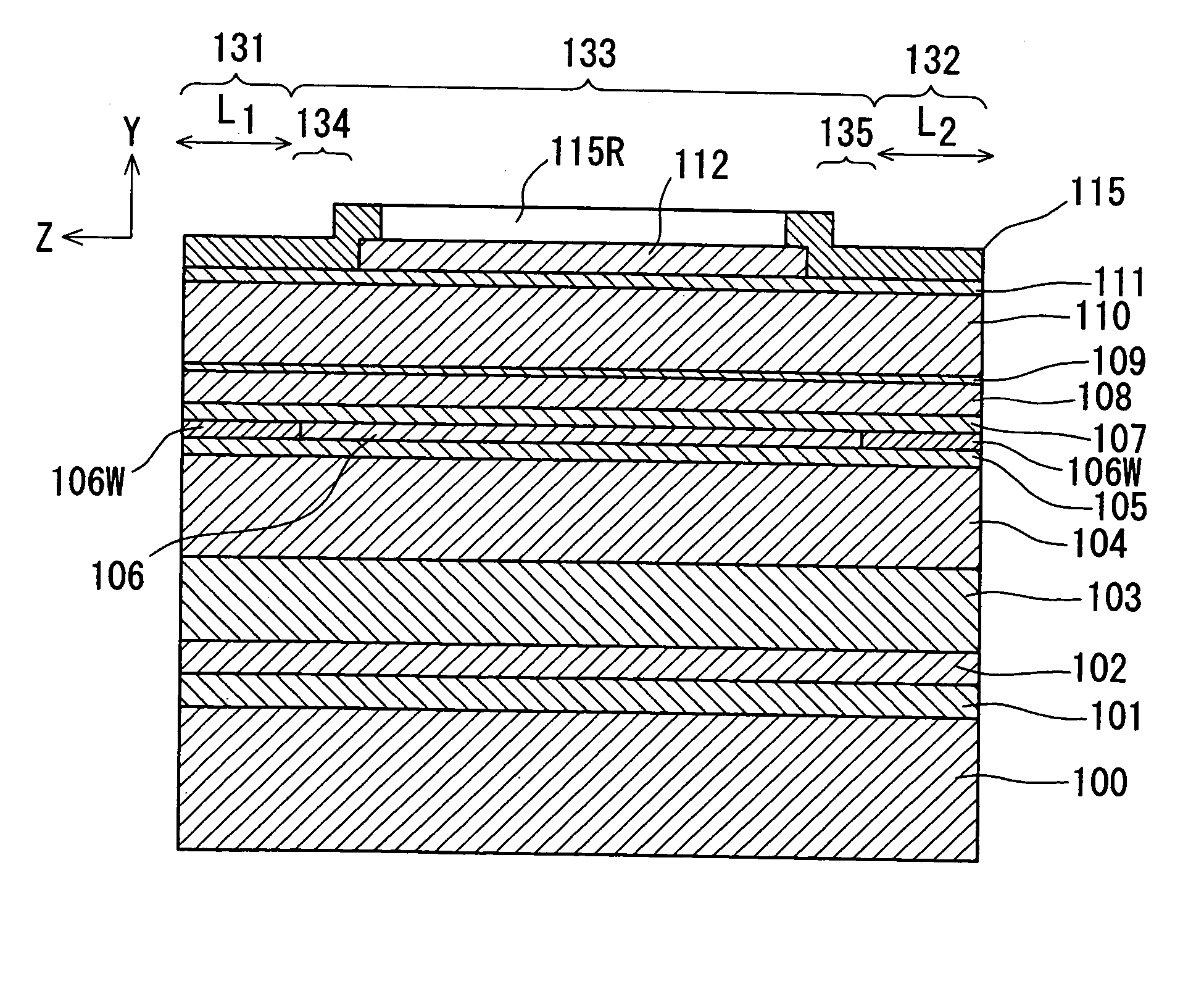
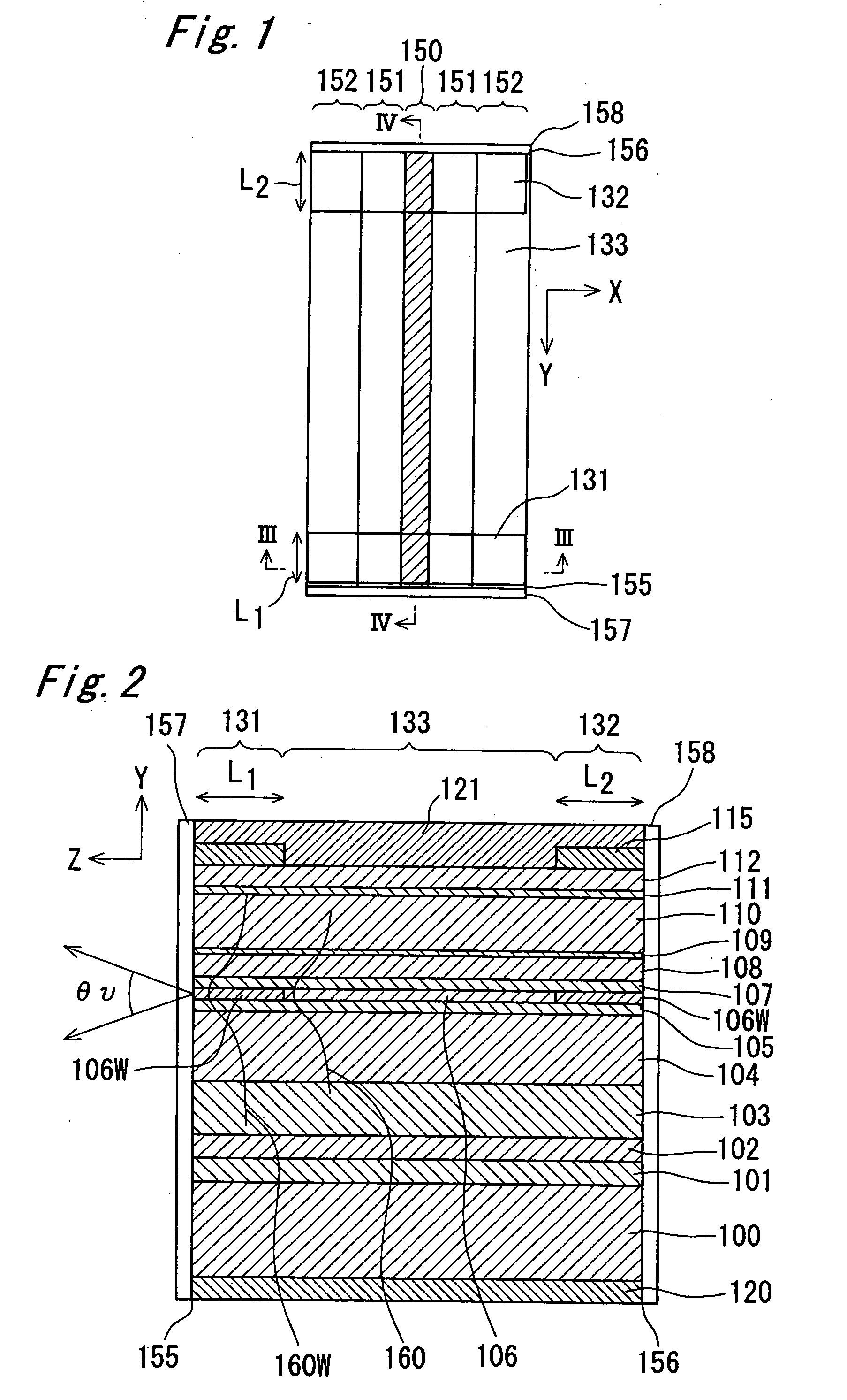
[0085] The structure of the semiconductor laser of the present embodiment is described. As shown in FIG. 1 that is a schematic top view, in the semiconductor laser of the present embodiment, a ridge region 150, a ridge side region 151 and a terrace region 152 are formed, and light is distributed in a region centered on an undoped MQW layer 106 (described later) located at the ridge region 150 and its neighborhood. A window portion 131 and a window portion 132 are formed within a range of L1 (60 μm) and L2 (60 μm) from a light-emitting end surface 155 and a rear end surface 156, respectively, and the other region serves as a non-window portion 133. A front antireflection coating 157 and a rear reflection coating 158 are formed on the light-emitting end surface 155 and the rear end surface 156, respectively.

[0086]FIG. 2 shows a sectional view taken along the line IV-IV of the semiconductor laser shown in FIG. 1. In the semicon...

embodiment 2

[0116] (Structure of Semiconductor Laser of Embodiment 2)

[0117] The point that the structure of Embodiment 2 differs from that of Embodiment 1 is described. In Embodiment 2, in reference to FIG. 1 that is the top view, the window lengths L1 and L2 are set to 70 μm. Moreover, in reference to FIG. 2 that is the sectional view, the undoped MQW layer 106 is formed by alternately layering six 3-nm thick Ga0.43In0.57P quantum well layers (106A, 106C, 106E, 106G, 106I, 106K) and five 5-nm (Al0.52Ga0.48)0.5In0.5P barrier layers (106B, 106D, 106F, 106H, 106J). The lower guide layer 105 and the upper guide layer 107 were made to have a thickness of 0.005 μm.

[0118] In Embodiment 2, by changing the quantum well layers in the undoped MQW layer 106 into 106A, 106C, 106E, 106G, 106I and 106K of which the layer thickness is 3 nm and increasing the number of quantum well layers from four to six, the sum quantum well layer thickness is made almost equalized, so that the optical confinement coeffici...

embodiment 3

[0124] (Structure of Semiconductor Laser of Embodiment 3)

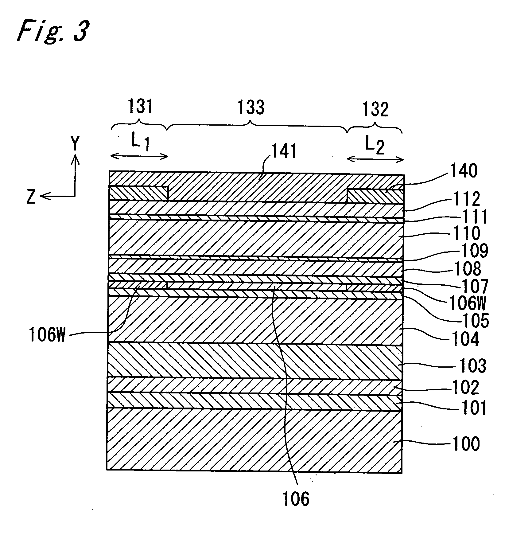
[0125] The point of the structure of Embodiment 3 different from that of Embodiment 1 is described. In Embodiment 3 as shown in FIG. 16 that is a sectional view in a manufacturing process, the window lengths L1 and L2 are set to 50 μm. Moreover, extended current non-injection regions 134 and 135 are provided as described later. The undoped MQW layer 106 is formed by alternately layering three 6-nm thick Ga0.48In0.52P quantum well layers (106A, 106C, 106E) and two 5-nm thick (Al0.52Ga0.48)0.5In0.5P barrier layers (106B, 106D). The thickness of the lower guide layer 105 and the upper guide layer 107 was set to 0.015 μm.

[0126] (Manufacturing Method of Semiconductor Laser of Embodiment 3)

[0127] The point of the manufacturing method of Embodiment 3 different from that of Embodiment 1 is described. First annealing is carried out in the state of the manufacturing process shown in FIG. 3. In the step, the atomic concentration of th...


PUM


Abstract

An AlGaInP based window structure semiconductor laser device of the present invention has an optical waveguide in which a lower cladding layer, an active layer having a quantum well layer, and an upper cladding layer are laminated in this order and which emits light from a light-emitting end surface that is formed on an end of the optical waveguide. A window portion having an active layer in which the quantum well layer is disordered is formed in an end portion including the light-emitting end surface in the optical waveguide. A light intensity distribution in a vertical direction for the laminated layers in the window portion spreads further than a light intensity distribution in the vertical direction in a non-window portion which is adjacent to the window portion inside the optical waveguide. A length of the window portion from the light-emitting end surface to the non-window portion is not smaller than 48 μm and not greater than 80 μm.

Description

CROSS-REFERENCE TO RELATED APPLICATIONS [0001] This Nonprovisional application claims priority under 35 U.S.C. §119(a) on Patent Application No. 2005-085903 filed in Japan on Mar. 24, 2005, the entire contents of which are hereby incorporated by reference. BACKGROUND OF THE INVENTION [0002] The present invention relates to window structure semiconductor laser devices and manufacturing methods therefor and relates, in particular, to a window structure semiconductor laser device capable of operating with a high output suitable for use in writing data into an optical disk such as DVD (Digital Versatile Disc) and reading data from an optical disk (hereinafter referred to as “for optical disk use”) and a manufacturing method therefor. [0003] As a semiconductor laser for optical disk use, an end surface emission type semiconductor laser is normally used. The semiconductor laser for optical disk use needs to have a laser beam capable of obtaining a spot shape as close as possible to the co...

Claims


Application Information

Patent Timeline
Patent Type & Authority Applications(United States)
IPC IPC(8): H01S3/08
CPCB82Y20/00H01S5/028H01S5/162H01S5/168H01S5/2214H01S5/2231H01S5/305H01S5/3063H01S5/34326H01S5/3436H01S2301/185
Inventor WATANABE, MASANORI
Owner SHARP KK
Why Eureka
Try Eureka